pcbComponent
Description
Use the pcbComponent
object to create a multiport PCB component
consisting of metal and dielectric layers.
Creation
Description
pcb = pcbComponent
creates a default PCB component.
pcb = pcbComponent(
sets Properties using one or more
name-value arguments. For example, PropertyName=Value
)pcb =
pcbComponent(Name='PCBWilkinson')
creates a PCB component named
'PCBWilkinson'
. Properties not specified retain their default
values.
pcb = pcbComponent(catalogcomponent)
creates a
pcbComponent
object from a PCB Components Catalog component. For
example, pcb = pcbComponent(microstripLine)
creates a
pcbComponent
from a microstripLine
catalog
component.
Properties
Name of the PCB component, specified a character vector or string scalar.
Example: component =
pcbComponent(Name='PCBsplitter')
Data Types: char
| string
Design revision details of the PCB component, specified as a character vector or string scalar.
Example: component = pcbComponent(Revision='v2.0')
Data Types: char
| string
Shape of the PC board, specified as a shape object. You can specify any one of the shapes from Custom Geometry and PCB Fabrication.
Example: trace = tracerectangular; component =
pcbComponent(BoardShape=trace)
creates a rectangle shaped trace on a
PCB.
Data Types: char
| string
Height of the PCB component, specified as a positive scalar in meters. To understand
more about BoardThickness
, see Board Thickness versus Dielectric Thickness in PCB.
Example: component =
pcbComponent(BoardThickness=0.0026)
Data Types: double
Metal and dielectric layers, specified a cell array of metal and dielectric layers. You can specify one metal shape or one dielectric substrate per layer starting with the top layer and proceeding downward.
Data Types: cell
Feed locations on the PCB component in Cartesian coordinates, specified as either an N-by-3 or N-by-4 array with N representing the number for ports on the PCB component. You can place the feed inside the board or at the edge of the board. The arrays translate into the following:
N-by-3 – [x, y, Layer]
N-by-4 – [x, y, SigLayer, GndLayer]
Example: component = pcbComponent(FeedLocations=[-0.0187 0 1
2])
Data Types: double
Diameter of center pin of the feed connector, specified as a positive scalar in meters.
Example: component =
pcbComponent(FeedDiameter=2.000e-04)
Data Types: double
Electrical short locations on the PCB component in Cartesian coordinates, specified as a real vector of size M-by-4 array. The array translates into the following:
M-by-4 – [x, y, SigLayer, GndLayer]
Example: component = pcbComponent(ViaLocations=[0 -0.025 1
2])
Data Types: double
Diameter of electrical shorting pin used between metal layers, specified as a positive scalar in meters for a single pin or a positive vector in meters for multiple pins. Number of values specified in this property must match the number of pins.
Example: component =
pcbComponent(ViaDiameter=1.0e-3)
Data Types: double
Model used for approximating the feed and the via, specified as one of the following:
'strip'
– A rectangular strip approximation to the feed and via cylinder. This approximation is the simplest and results in a small mesh.'square'
– A four-sided polyhedron approximation to the feed and via cylinder.'hexagon'
– A six-sided polyhedron approximation to the feed and via cylinder.'octagon'
– An eight-sided approximation to the feed and via cylinder.
Example: component=pcbComponent(FeedViaModel='square')
Data Types: string
| char
Type of metal used in conducting layers, specified as a metal object. For more
information see metal
.
Example: m=metal('Copper');
component=pcbComponent(Conductor=m)
Data Types: metal object
Lumped elements added to the PCB component feed, specified as a lumped element
object handle. For more information, see lumpedElement
(Antenna Toolbox).
Example: p=pcbComponent;p.Load=lumpedElement;
Angle of component tilt, specified in degrees, around the Z axis.
Example: component=pcbComponent(Tilt=30)
Data Types: double
Tilt axis of a PCB component, specified as [0 0 1]
or
'Z'
.
Note
Only the Z axis is currently supported.
Example: pcb.TiltAxis = 'Z'
Data Types: double
Specifies whether the FeedLocations
property, or the
FeedDefinitions
property is used to configure the feeds of the
pcbComponent
object.
Example: p=pcbComponent;p.FeedFormat='FeedDefinitions'
Data Types: char
| string
Specifies feed types used in a pcbComponent
object.
Feed Definitions
Type | Applications | Usage |
---|---|---|
ArbitraryFiniteGapFeed | Construct a complicated feed in which one or more signal locations must be excited positively with respect to one or more ground locations. | |
ProbeFeed | Microstrip patch antennas; vertical launch feed | Construct a via of cross section specified by Apply excitation at the
|
EdgeFeed | Microstrip elements whose signal originates on the PCB edge with one ground plane. Stripline elements with two ground planes. | Define a positive feed edge on the metal edge passing through
SignalLocations(x,y) on the SignalLayer ;
define negative feed edges on all metal edges passing through Location (x, y) on
all specified GroundLayers . |
DeltaGapFeed | Balanced structures, dipole antennas, lumped loads | Create a delta-gap feed of width
|
CoaxialFeed | Higher-fidelity version of a probe feed | Create a via of arbitrary shape specified by
Define the positive feed edge
along the entire perimeter of The The |
FiniteFeedGap | Coplanar multi-ground edge feeds, finite-width delta-gap feeds | On the layer specified by SignalLayer , place positive
feed edges at each of the N metal edge sites specified by
SignalLocations . On the same layer, place negative feed
edges at each of the N metal edge sites specified by
GroundLocations . Feed n (ε 1:N) has width
SignalWidths(n) . |
Note
FeedDefinitions
objects are only accessible when the
FeedFormat
property is set to
'FeedDefinitions'
Example: p=pcbComponent;p.FeedFormat='FeedDefinitions';p.FeedDefinitions=DeltaGapFeed('SignalLocations',[0
0],'SignalWidths',p.Layers{1}.Width,'SignalLayers',1);
Data Types: FeedDefinitions object
The type of solver used for component analysis, specified as a string: either method
of moments ('MoM'
), or finite element method
('FEM'
). For more information on solvers see Overview of Solvers.
Example: component=pcbComponent(SolverType='FEM')
Note
To enable FEM solver required for the metal shield property, download the
Integro-Differential Modeling Framework for MATLAB
. To download
this add-on:
In the Home tab Environment section, click on Add-Ons. This opens the add-on explorer. You need an active internet connection to download the add-on.
Search for
Integro-Differential Modeling Framework for MATLAB
and click Install.To verify if the download is successful, run
in your MATLAB® session command line.matlab.addons.installedAddons
On Windows, to run the IDMF add-on, you must install the Windows Subsystem for Linux (WSL). To install WSL, see Install Linux on Windows with WSL.
The Windows Defender Firewall can block the PostgreSQL server when using the IDMF add-on. To resolve this issue, you can allow the server to communicate on desired networks if the firewall prompts. Alternatively, you can manually add the executable file of the PostgreSQL server located in
<matlabroot>\sys\postgresql\win64\PostgreSQL\bin\postgres.exe
. For more information, see https://support.microsoft.com/en-us/windows/risks-of-allowing-apps-through-windows-defender-firewall-654559af-3f54-3dcf-349f-71ccd90bcc5c.
Note
Use the solver
object to set the properties of the FEM solver. SolverType
must
be specified as'FEM'
.
Data Types: string
Connector specifies the type of RF connector assembled at the feed locations of the
pcbComponent
, as a RFConnector
object. The
SolverType
must be set to 'FEM'
to enable this
property.
Example: component=pcbComponent(SolverType='FEM',
Connector=RFConnector)
Data Types: RFConnector object
Flag to add a metal shielding to the PCB component, specified as a logical 0 or logical 1. The default value is logical 0.
Example:
IsShielded = true
or 1
add a metal
shield.
Note
To enable FEM solver required for the metal shield property, download the
Integro-Differential Modeling Framework for MATLAB
. To download
this add-on:
In the Home tab Environment section, click on Add-Ons. This opens the add-on explorer. You need an active internet connection to download the add-on.
Search for
Integro-Differential Modeling Framework for MATLAB
and click Install.To verify if the download is successful, run
in your MATLAB session command line.matlab.addons.installedAddons
On Windows, to run the IDMF add-on, you must install the Windows Subsystem for Linux (WSL). To install WSL, see Install Linux on Windows with WSL.
The Windows Defender Firewall can block the PostgreSQL server when using the IDMF add-on. To resolve this issue, you can allow the server to communicate on desired networks if the firewall prompts. Alternatively, you can manually add the executable file of the PostgreSQL server located in
<matlabroot>\sys\postgresql\win64\PostgreSQL\bin\postgres.exe
. For more information, see https://support.microsoft.com/en-us/windows/risks-of-allowing-apps-through-windows-defender-firewall-654559af-3f54-3dcf-349f-71ccd90bcc5c.
Data Types: boolian
This property is read-only.
Metal shield for the PCB component, specified as a shape.Box
object.
The length and width of the box must be equal to the length and width of the ground plane.
The center of the box is at [0 0 Shielding.Height]
.
Dependencies
To enable the Shielding
property, set the
IsShielded
property to true
or
1
.
Object Functions
current | Calculate and plot current distribution |
charge | Calculate and plot charge distribution |
feedCurrent | Calculate current at feed port |
gerberWrite | Generate Gerber files |
layout | Plot all metal layers and board shape |
mesh | Change and view mesh properties of metal or dielectric in PCB component |
meshconfig | Change mesh mode of PCB component or shape structure |
sparameters | Calculate S-parameters for RF PCB objects |
show | Display PCB component structure or PCB shape |
pcbcascade | Create new component using cascade operation |
solver | Access FEM solver settings for electromagnetic analysis |
Examples
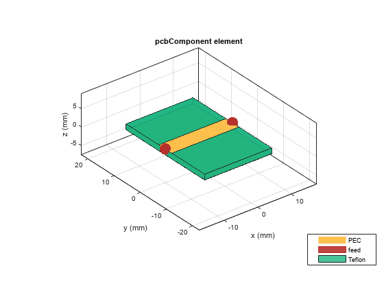
Create a PCB component using default properties.
pcb = pcbComponent;
View the PCB component.
show(pcb)
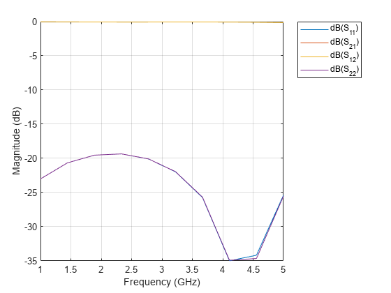
Calculate S-parameters over 10 frequencies from 1-5 GHz.
s=sparameters(pcb,linspace(1e9,5e9,10));
Plot the S-parameters.
rfplot(s)
Create a PCB component with a lid at a distance of 2 cm above the component.
p = pcbComponent;
pcblid = traceRectangular(Length=p.Layers{1}.Length,Width=p.Layers{3}.Width);
dAir = dielectric('Air');
dAir.Thickness = 2e-2;
p.BoardThickness = p.BoardThickness + dAir.Thickness;
p.Layers = {pcblid,dAir,p.Layers{1},p.Layers{2},p.Layers{3}};
p.FeedLocations(:,3:4) = [3 5;3 5];
show(p)
Calculate the S-parameters over the 10 frequencies from 1-5 GHz.
s = sparameters(p,linspace(1e9,5e9,10)); rfplot(s)
Version History
Introduced in R2021bUse the FeedFormat
and FeedDefinitions
properties
to define and create six types of feeds.
See Also
gerberRead
| gerberWrite
| PCBReader
| PCBWriter
| PCBServices
| dielectric
MATLAB Command
You clicked a link that corresponds to this MATLAB command:
Run the command by entering it in the MATLAB Command Window. Web browsers do not support MATLAB commands.
Select a Web Site
Choose a web site to get translated content where available and see local events and offers. Based on your location, we recommend that you select: United States.
You can also select a web site from the following list
How to Get Best Site Performance
Select the China site (in Chinese or English) for best site performance. Other MathWorks country sites are not optimized for visits from your location.
Americas
- América Latina (Español)
- Canada (English)
- United States (English)
Europe
- Belgium (English)
- Denmark (English)
- Deutschland (Deutsch)
- España (Español)
- Finland (English)
- France (Français)
- Ireland (English)
- Italia (Italiano)
- Luxembourg (English)
- Netherlands (English)
- Norway (English)
- Österreich (Deutsch)
- Portugal (English)
- Sweden (English)
- Switzerland
- United Kingdom (English)