Custom Geometry and PCB Fabrication
R2026bUse the shape objects to create different designs and complex shapes and create custom printed circuit board (PCB) components to complete PCB designs quickly. Use line interconnects such as bends, curves, mitered edges, and traces to effectively lay out PCB components.
Gerber files are open ASCII vector format files that contain information on each physical board layer of the PCB design. These files also represent circuit board objects, like copper traces, vias, pads, solder mask, and silkscreen images by series of coordinates. Write Gerber files that can be used by PCB manufacturers to translate the details of the design into physical properties of the PCB.
Apps
| PCB VIEWER | Import, visualize, inspect, and navigate printed circuit boards (Since R2026a) |
Objects
Functions
Topics
- Board Thickness Versus Dielectric Thickness in PCB
This example shows you how to define the BoardThickness of PCB with respect to dielectric thickness of
pcbComponentobject for different use-cases.
Featured Examples
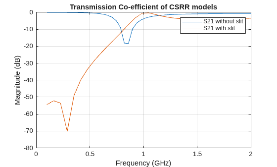
Create and Analyze Dual Characteristics of Complementary Split Ring Resonators from Gerber Files
Create and analyze of complementary split ring resonators from Gerber files.
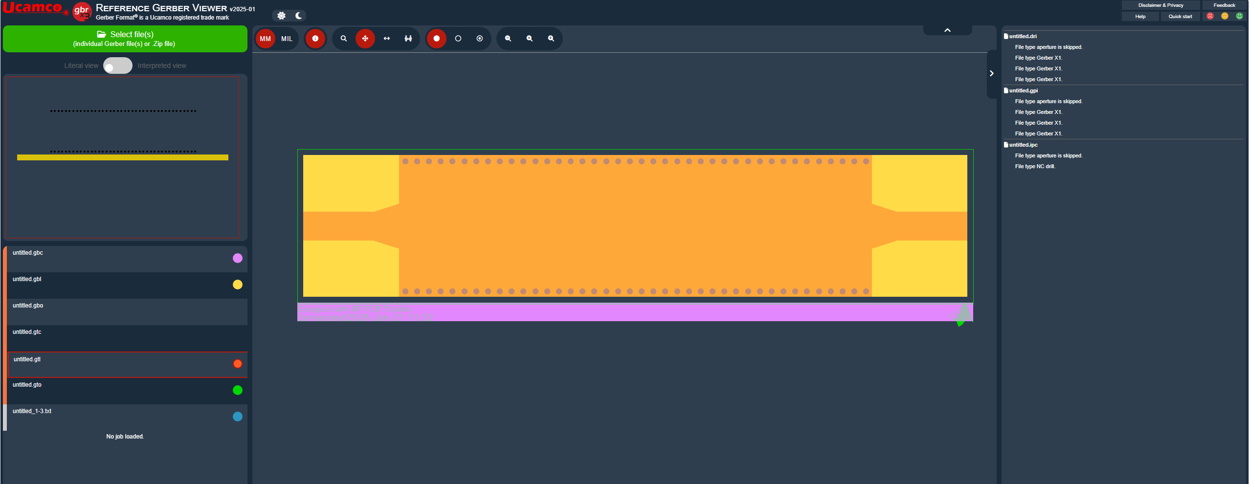
Prototype, Design, and Analysis of SIW based Microstrip Tapered Transmission Line
Design and analyze SIW transmission line.
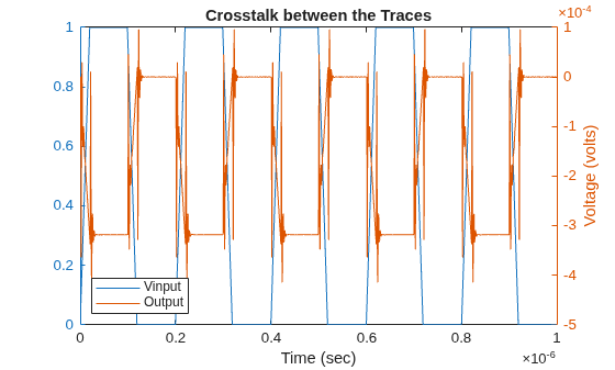
Analyzing Crosstalk Between PCB Traces
Analyze crosstalk between PCB traces.
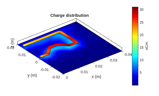
Create and Analyze PCB Interconnects Using Custom Traces
Create and analyze PCB traces.
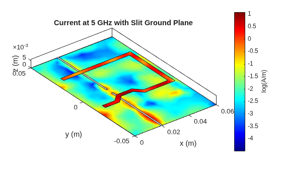
Routing Discipline to Reduce Crosstalk
Analyze surface currents and follow routing discipline on a PCB trace.
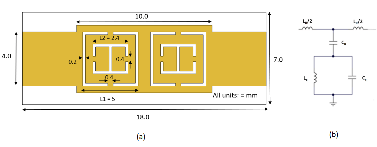
Design and Analyze Compact UWB Low Pass Filter Using pcbComponent
Design and analyze a compact low pass ultra-wide band (UWB) filter based on a U-shaped complementary split ring resonator using the pcbComponent object. The filter is designed to have very low insertion loss over a wide band of frequency from low 0.1 GHz to 10.8 GHz. The design of the filter is taken from the reference [1].
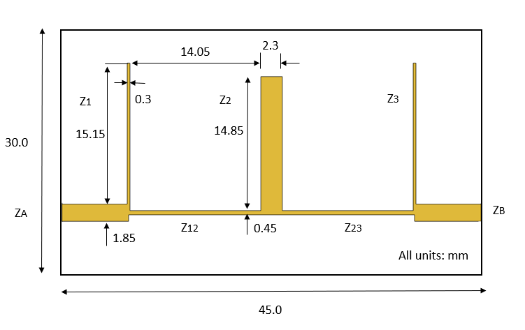
Design and Analyze Band Stop Filter Using pcbComponent
Design and analyze band stop filter using the pcbComponent object. Design the band stop filter with a fractional bandwidth (FBW) of 1.0 at a midband frequency f0 of 2.5 GHz for the band-edge frequencies of f1 = 1.25 GHz and f2 = 3.75 GHz as defined in Figure 6.11b of reference [1].
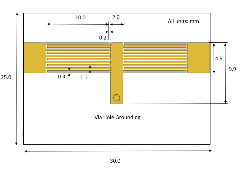
Design and Analyze HighPass Filter Using pcbComponent
Design and analyze highpass filter using the pcbComponent object. A microstrip highpass filter is designed based on a three-pole (n = 3) Chebyshev highpass prototype with 0.1 dB passband ripple and cutoff frequency fc = 1.5 GHz.

