Clock Skew in Synchronous Interface Timing
In a synchronous interface, data transfer occurs between a source device and a target device that share a common clock distribution. The difference in time between when the clock arrives at the clock pins of the target and source devices is known as clock skew. There are two types of clock skew:
Setup Skew — The earliest target clock minus the latest source clock (minimum target – maximum source). Negative values of setup skew reduce setup margin.
Hold skew — The latest target clock minus the earliest source clock (maximum target – minimum source). Positive values of hold skew reduce hold margin.
The basic equations that govern the setup and hold timing margin calculation include the delay (Tco) values of the driving chip, setup and hold constraints on the target chip, etch delays, and clock skews.
In the Parallel Link Designer app, you can calculate clock skew for synchronous designs using two methods:
Dynamic Clock Skew — Use the pin-to-pin clock skews and interconnect delays to calculate the skew between the source clock and the target clock.
User-Defined Clock Skew — Define a value in the clock skew text file.
Note
When both dynamic and user-defined clock skew data are present, dynamic clock skew calculation takes precedence over user-defined clock skews.
Dynamic Clock Skew
Dynamic clock skew calculation is the most accurate method to determine the clock skew between the clock pins that are sourced by a common clock buffer device.
To calculate the dynamic skew, you must create the appropriate transfer net sheets
between the clock buffer device and the clocked device. The timing model for the clock
buffer must have a CLOCK_SKEW statement between the output clock
PINDEFs to define the timing relationship between these output pins.
All output clock pins can be in the same PINDEF and the
CLOCK_SKEW statement can reference that PINDEF to
itself.
You can also set cycle-to-cycle jitter on the clock transfer nets. Jitter affects the setup margins for synchronous common-clock systems.
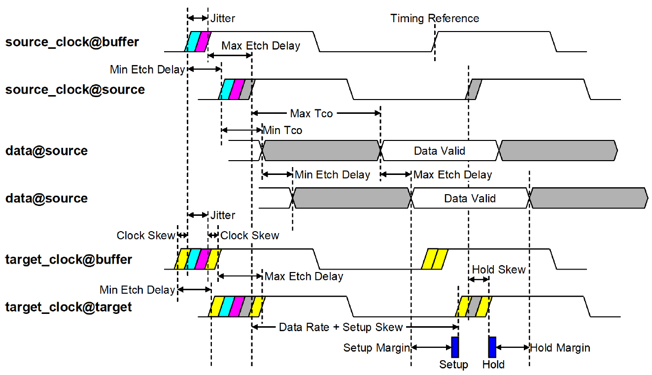
The Parallel Link Designer app calculates the dynamic clock skew on a corner-by-corner basis. The app combines the clock skew between the output clock pins with jitter and interconnect delays to dynamically compute the worst-case setup skew and hold skew. It does not combine the cross corner interconnect delays for a source clock and target clock (FFFE and SSSE) to calculate setup and hold skews; because the clock distribution network cannot be simultaneously fast and slow. Only one setup skew and one hold skew are used for synchronous analysis. The worst case of FFFE and SSSE is used for setup and hold margin analysis.
The app computes the setup and hold skews independently on rising and falling clock edges, solution space cases and corners:
Parameters in Clock Skew Calculation
| Parameter | Description |
|---|---|
| UI | Defined in the transfer net of the data signal. |
| Jitter | Defined in the transfer net of the clock signal. |
| Min Tco | Defined in the timing model of the source device. |
| Max Tco | |
| Setup | Defined in the timing model of the target device. |
| Hold | |
| Min Data Etch Delay | Determined from the simulation during the waveform analysis. |
| Min Data Etch Delay | |
| Setup Skew | The clock skew condition that creates the worst case setup margin. It is determined from the latest source clock and earliest target clock. Negative setup skew reduces setup margin. |
| Hold Skew | The clock skew condition that creates the worst case hold margin. It is determined from the earliest source clock and latest target clock. Positive hold skew reduces hold margin. |
| Min Source Clock Etch Delay | Determined from the simulation during the waveform analysis for dynamic clock skew calculation. |
| Max Source Clock Etch Delay | |
| Min Target Clock Etch Delay | |
| Max Target Clock Etch Delay | |
| Clock Skew Min | Defined in the timing model for the device driving the clocks. |
| Clock Skew Max |
The relationship between the different timing parameters can be shown in a timing diagram:
Example of Dynamic Clock Skew Calculation
You can calculate dynamic clock skew from the given timing parameters:
CLOCK_SKEWstatement for clock buffer has ±0.25 ns skew.Source Clock Etch Delays: Rmin = –0.167 ns, Rmax= –0.031 ns.
Target Clock Etch Delays: Rmin = –0.167 ns, Rmax= –0.031 ns.
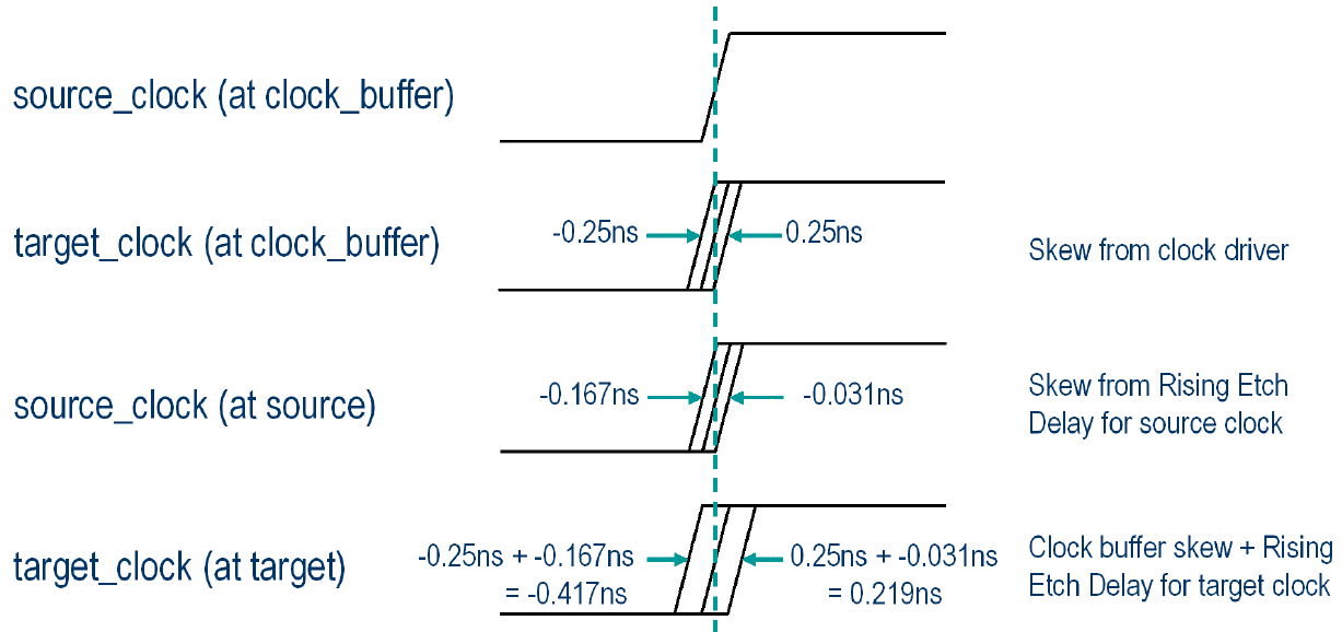
So, the setup skew is the earliest target clock (–0.417 ns) minus latest source clock (–0.031 ns) which results in –0.386 ns.
And the hold skew is the latest target clock (0.219 ns) minus earliest source clock (–0.167 ns) which results in 0.386 ns.
User-Defined Clock Skew
The Parallel Link Designer app supports user-defined clock skews to allow explicit definition of the setup skew and hold skew between state devices. In this case. the clock nets are not present or not simulated. This is the simplest way to specify a synchronous clock skew value.
To define the clock skew, access the clock skew file from Setup > Clock Skew in the app toolstrip.
Synchronous interfaces require the source device to have a timing model with a
DELAY statement between the clock and output pins. The target device
must have SETHLD constraints between the clock and signal input pins.
Clock skew is always defined as the worst-case difference between the time the clock arrives
at the target clock pin and the source clock pin. It should account for all variations in
the clock distribution system that can add uncertainty or offsets to one clock pin with
respect to the other.
User-Defined Clock Skew Syntax
The general syntax for defining clock skew in the clock skew file is:
<SourceClkPin> <TargetClkPin> <SetupSkew> <HoldSkew>
| Keyword | Description |
|---|---|
<SourceClkPin> | The clock pin on the source device. DELAY statements in
the timing model of the device define the relationship between the clock pin and
the output pins. You must define separate skew statements for each source clock
pin. |
<TargetClkPin> | The clock pin on the target device. SETHLD (Setup/Hold)
constraints in the timing model of the device define the required timing
relationship between the clock pin and associated input pins. You must define
separate skew statements for each target clock pin. |
<SetupSkew> | The worst-case difference between the earliest target clock and the latest
source clock. Positive setup skew indicates that the clock arrives at
<TargetClkPin> after it arrives at
<SourceClkPin> under worst-case conditions. |
<HoldSkew> | The worst-case difference between the latest target clock and the earliest
source clock. Positive hold skew indicates that the clock arrives at
<TargetClkPin> after it arrives at
<SourceClkPin> under worst-case conditions. |
You can define the <SourceClkPin> and
<TargetClkPin> in any of these five formats:
<part_name>/<pinname>
<designator>/<pinname>
<designator>/<part_name>/<pinname>
<reference_designator>.<pinumber>
<board_id>/<reference_designator>.<pinumber>
The format used for <SourceClkPin> and
<TargetClkPin> must be the same.
<part_name> | Parallel Link Designer part name defined in the part library. |
<pinname> | The logical pin name for the source clock pin or target clock pin as it appears in both the IBIS and timing models. |
<designator> | The designator name of the driver or receiver in the sheet for the source or target device. An interface can have multiple sheets, each of which may refer to a designator using a different name. |
<reference_designator> | The unique part identifier in the CAD/layout database. |
<pinnumber> | The physical pin number associated with the specific reference designator. |
<board_id> | The unique board name associated with the CAD/layout database during the Board Extraction and Assignment process. |
User-Defined Clock Skew Example
You can define a clock skew using the part name and pin name syntax. The clock signal
at sdram/clk can trigger from 400ps before to 300ps after the clock
signal at northbridge/clock.
partname/pinname partname/pinname SetupSkew (ns) HoldSkew (ns)
sdram/clk northbridge/clock -0.4 0.3
northbridge/clock sdram/clk -0.3 0.4
You can include two memory devices, each of which has a different static clock offset, but the same width (early/late) clock window. This uses the designator, part name, and pin name syntax.
designator/partname/pinname designator/partname/pinname SetupSkew HoldSkew
sdram1/sdram/clk northbridge/northbridge/clock -0.42 0.28
northbridge/northbridge/clock sdram1/sdram/clk -0.28 0.42
sdram2/sdram/clk northbridge/northbridge/clock -0.37 0.33
northbridge/northbridge/clock sdram2/sdram/clk -0.33 0.37
You can define skew for post-layout analysis using reference designator and pin number syntax:
ref_des.pinnumber ref_des.pinnumber SetupSkew (ns) HoldSkew (ns)
U2.B30 U3.23 -0.42 0.28
U3.23 U2.B30 -0.28 0.42
U2.B30 U4.23 -0.37 0.33
U4.23 U2.B30 -0.33 0.37
You can also define clock skew for post-layout using board ID, reference designator, and pin number syntax:
board_id/ref_des.pinumber board_id/ref_des.pinumber SetupSkew HoldSkew
motherboard/U2.B30 motherboard/U3.23 -0.42 0.28
motherboard/U3.23 motherboard/U2.B30 -0.28 0.42
motherboard/U2.B30 daughtercard/U4.23 -0.37 0.33
daughtercard/U4.23 motherboard/U2.B30 -0.33 0.37