Get Started with IP Core Generation for Microchip PolarFire SoC Devices
This example shows how to use the hardware-software co-design workflow to blink LEDs at various frequencies on the Microchip PolarFire® SoC Icicle kit.
Introduction
This example is a step-by-step guide that helps you use HDL Coder™ to generate a custom HDL IP core that blinks LEDs on the Microchip PolarFire SoC Icicle kit.
You can use MATLAB® and Simulink® to design, simulate, and verify your application, perform what-if scenarios with algorithms, and optimize parameters. You can then prepare your design for hardware and software implementation on the PolarFire SoC Icicle Kit by deciding which system elements are performed by the programmable logic, and which system elements are run on the RISC-V processor.
Using the guided workflow shown in this example, you automatically generate HDL code for the programmable logic by using HDL Coder and implement the design on the Microchip PolarFire SoC Icicle Kit.
In this workflow, you perform these tasks:
Set up your PolarFire SoC hardware and tools.
Partition your design for hardware and software implementation.
Generate an HDL IP core by using HDL Workflow Advisor.
Integrate the IP core into a Microchip Libero project and program the PolarFireSoC hardware.
Requirements
Microchip Libero Design Suite, with supported version listed in the HDL Language Support and Supported Third-Party Tools and Hardware.
Microchip PolarFire SoC Icicle Kit.
HDL Coder Support Package for Microchip FPGA and SoC Devices.
Set Up PolarFire SoC Hardware and Tools
1. Set up the Microchip PolarFire SoC Icicle Kit as shown in the figure. To learn more about the PolarFire SoC hardware setup, see PolarFire SoC Icicle Kit Quickstart Card.

Connect your computer to the USB UART connector by using a Micro-USB cable. Make sure that your USB device drivers, such as for the Silicon Labs CP210x USB to UART Bridge, are installed correctly. If not, search for the drivers online and install them.
2. Connect your computer and the PolarFire SoC board using an Ethernet cable.
3. Install the HDL Coder Support Packages for Microchip FPGA and SoC Devices if you have not already done so. To start the installer, on the MATLAB toolstrip, click Add-Ons > Get Hardware Support Packages. Search for HDL Coder Support Packages for Microchip FPGA and SoC Devices and install them.
4. Make sure that you are using the SD card image provided by Microchip from Github Link.
5. Set up the PolarFire SoC hardware connection in this MATLAB Command Window.
6. You can optionally test the serial connection by using the configuration that uses a program such as PuTTY™. Baud rate: 115200; Data bits: 8; Stop bits: 1; Parity: None; Flow control: None. You can see Linux® booting log on the serial console when you Power Cycle the PolarFire SoC board.
7. Set up the Microchip Libero SoC tool path by using hdlsetuptoolpath function in the MATLAB Command Window. When you run the command, use own Microchip Libero installation path.
hdlsetuptoolpath('ToolName', 'Microchip Libero SoC', 'ToolPath', liberopath);
Partition Your Design for Hardware and Software Implementation
For the PolarFire SoC hardware-software co-design workflow, decide which parts of your design to implement on the programmable logic and which parts to run on the RISC-V processor.
Group all the blocks that you want to implement on programmable logic into an atomic subsystem. This atomic subsystem is the boundary of your hardware-software partition. The blocks inside this subsystem are implemented on programmable logic and the blocks outside this subsystem run on the RISC-V processor.
In this example, the subsystem led_counter is the hardware subsystem. It models a counter that blinks the LEDs on an FPGA board. Two input ports, Blink_frequency and Blink_direction, are control ports that determine the LED blink frequency and direction. The blocks outside of the subsystem led_counter are for software implementation.
In Simulink, you can use the Slider Gain or Manual Switch block to adjust the input values of the hardware subsystem. In the embedded software, this means the RISC-V processor controls the generated IP core by writing to the AXI interface accessible registers. The output port of the hardware subsystem, LED, connects to the LED hardware. You can use the output port, Read_Back, to read data back to the processor.
open_system('hdlcoder_led_blinking_4bit');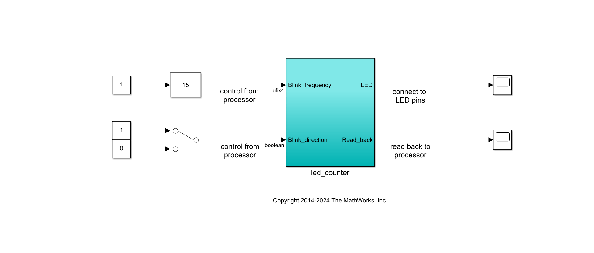
Generate HDL IP Core by using the HDL Workflow Advisor
You can generate a shareable and reusable IP core module from a Simulink model. The generated IP core connects to an embedded processor on an FPGA device. HDL Coder generates HDL code from the Simulink blocks and generates HDL code for the AXI interface logic connecting the IP core to the embedded processor. HDL Coder packages the generated files into an IP core folder. You can then integrate the generated IP core with a larger FPGA embedded design in the Microchip Libero environment.
Start IP Core Generation Workflow.
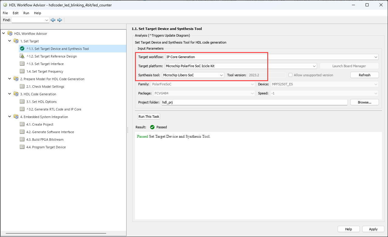
1. Select the hdlcoder_led_blinking/led_counter subsystem. On the Apps tab, click HDL Coder. On the HDL Code tab, in the Assistance section, click Workflow Advisor to open the HDL Workflow Advisor.
2. In the Set Target > Set Target Device and Synthesis Tool task, for Target workflow, select IP Core Generation.
3. For Target platform, select Microchip PolarFire SoC Icicle kit. If you don't have this option, select Get more to open the Support Package Installer.
4. Click Run This Task to run the Set Target Device and Synthesis Tool task.
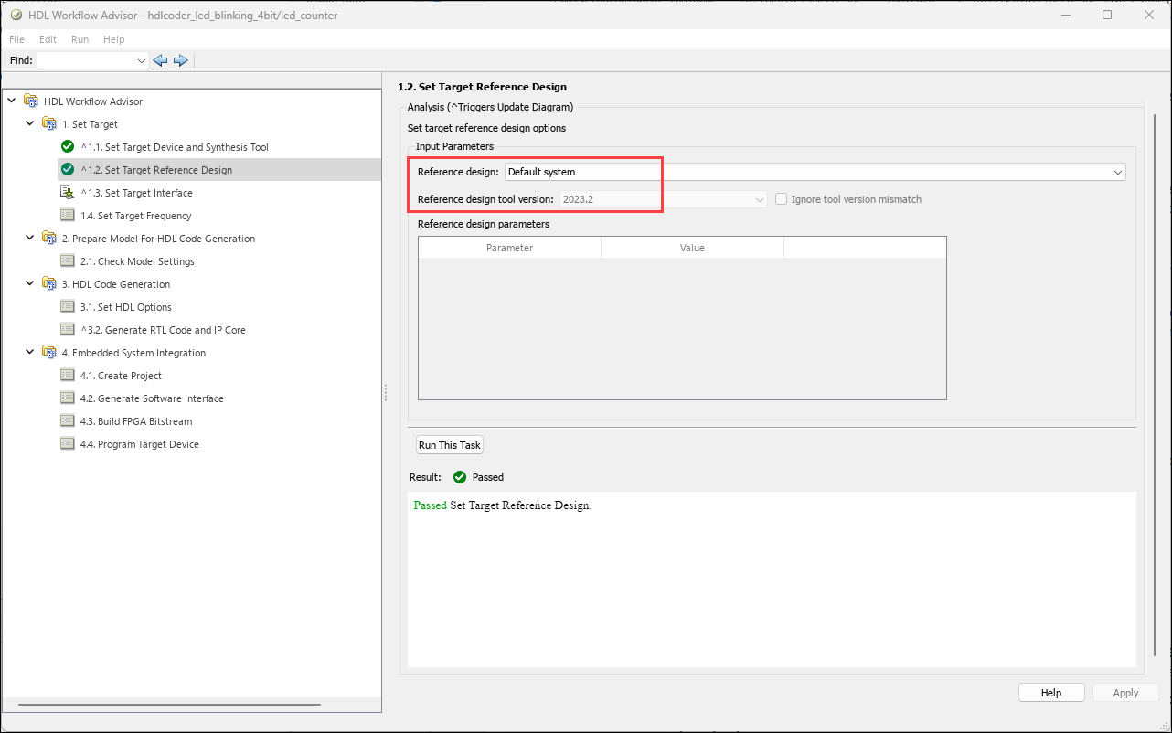
5. In the Set Target > Set Target Reference Design task, Reference Design Default system is selected by default.
6. Click Run This Task to run the Set Target Reference Design task.
Configure Target Interface.
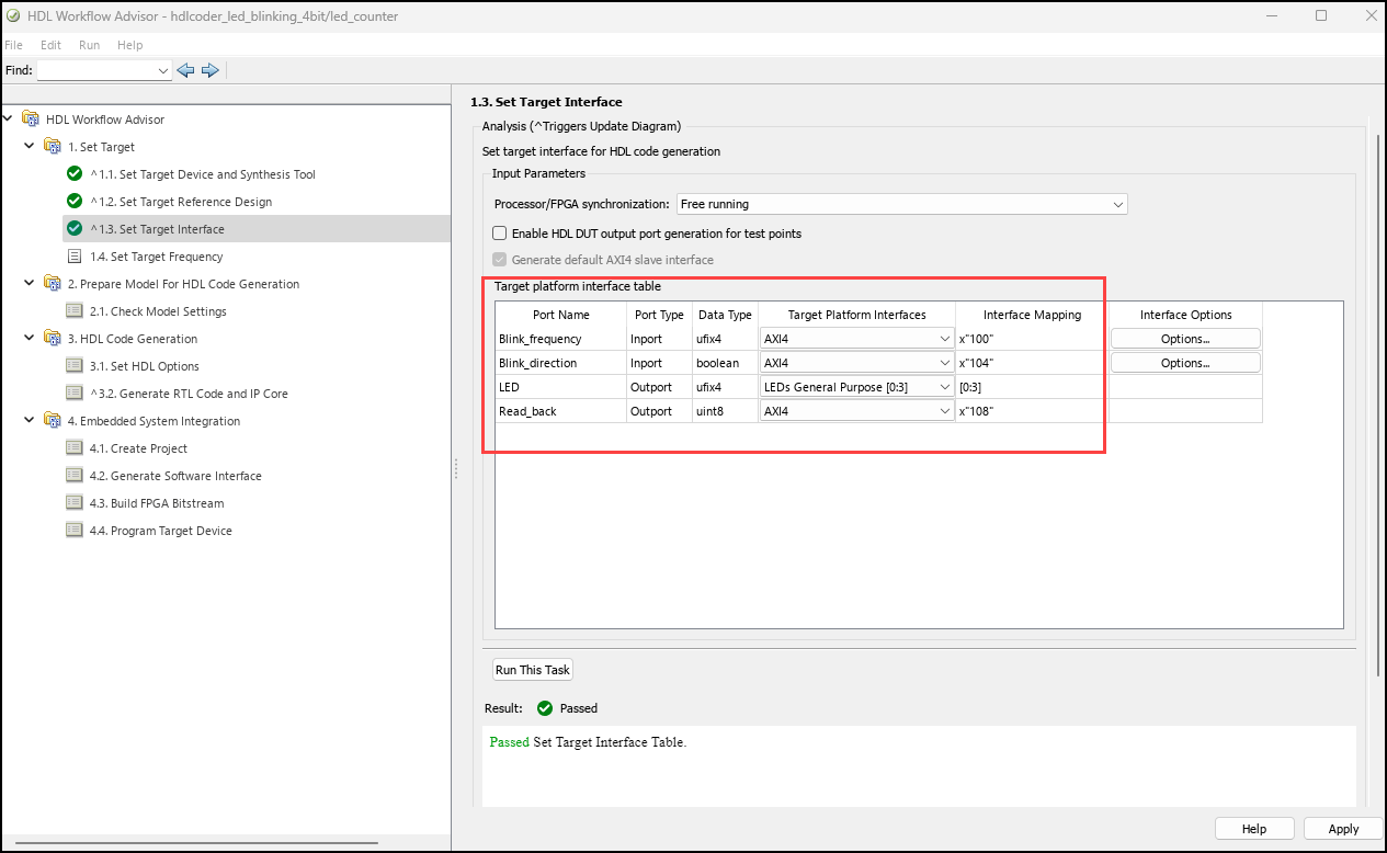
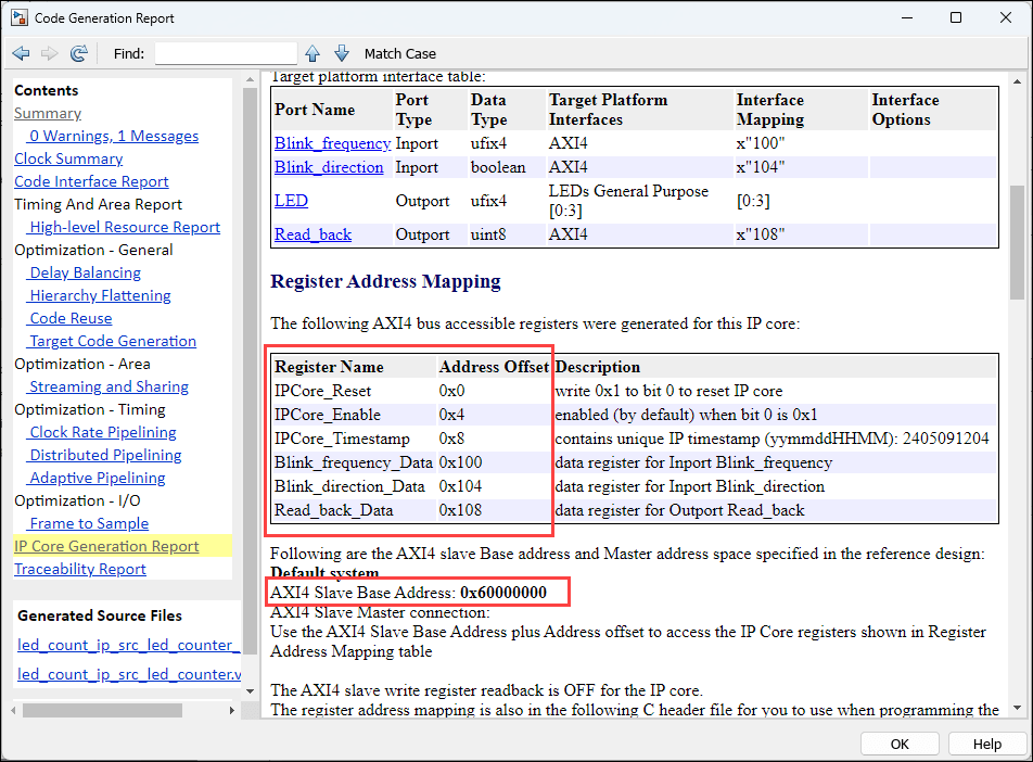
Map each port in your DUT to one of the IP core target interfaces. In this example, input ports Blink_frequency and Blink_direction are mapped to the AXI4 interface. HDL Coder generates AXI interface accessible registers for them. The LED output port is mapped to an external interface, LEDs General Purpose [0:3], which connects to the LED hardware on the PolarFire SoC board.
1. In the Set Target > Set Target Interface task, choose AXI4 for Blink_frequency, Blink_direction, and Read_back.
2. Choose LEDs General Purpose [0:3] for LED.
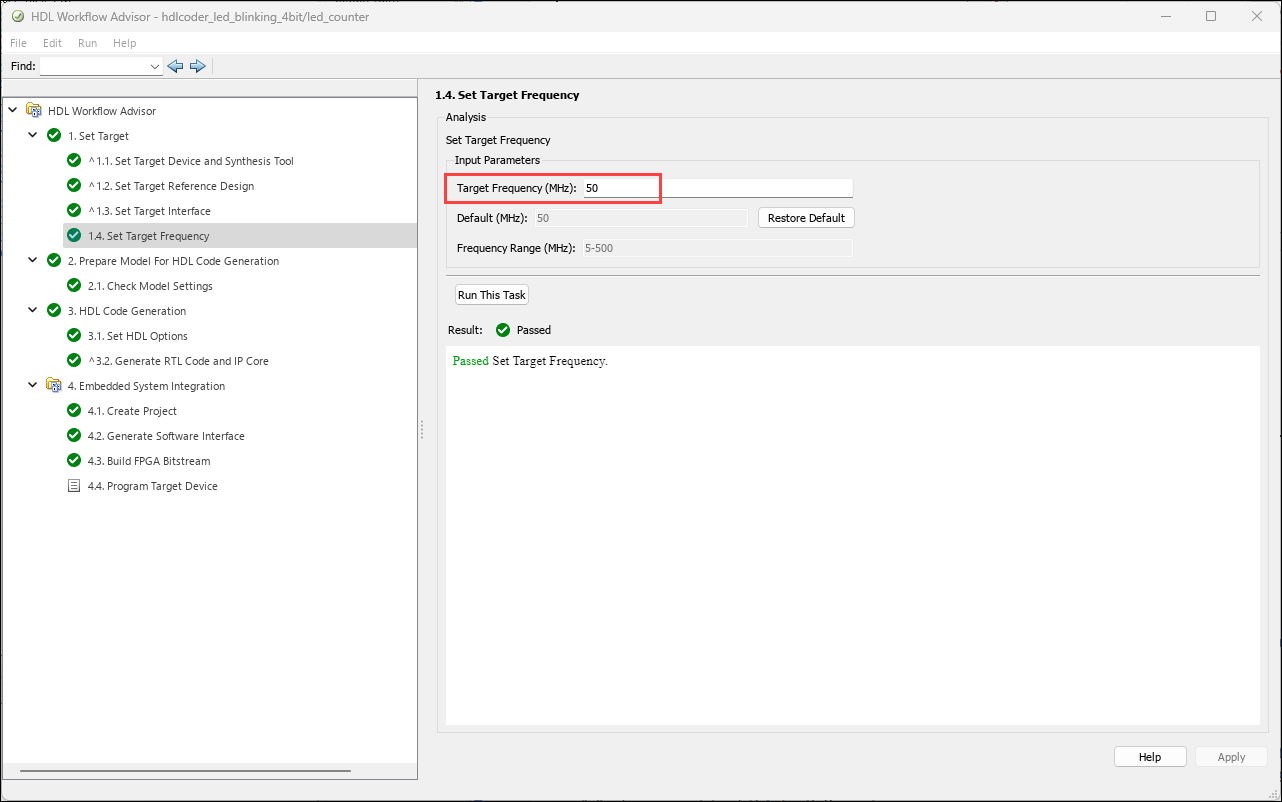
3. In the Set Target > Set Target Frequency task, set Target Frequency (MHz) to 50.
Generate IP Core
1. In the task 3.2 Generate RTL Code and IP Core, select Enable readback on write registers option to read from input registers. Right-click the Generate RTL Code and IP Core task and select Run to Selected Task.
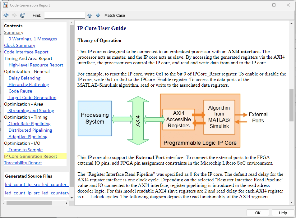
2. Generate and view the IP core report.
After you generate the custom IP core, the IP core files are in the ipcore folder within your project folder. An HTML custom IP core report is generated with the custom IP core. The report describes the behavior and contents of the generated custom IP core.
3. Register Address Mapping.
IP Core Generation Report also contains the details about Target Platform Interface of your model. The figure shows the AXI4 interface mapped to the hdlcoder_led_blinking_4bit model ports. The table in IP Core Generation Report shows the interface mapping address of each register. These addresses are used to read the input registers.

Integrate IP Core with Microchip Libero SoC Environment
Insert your generated IP core into an embedded system reference design, generate an FPGA bitstream, and download the bitstream to the PolarFire SoC hardware.
The reference design is a predefined Microchip Libero project. It contains the elements the Libero software requires to deploy your design to the PolarFire SoC board, except for the custom IP core.
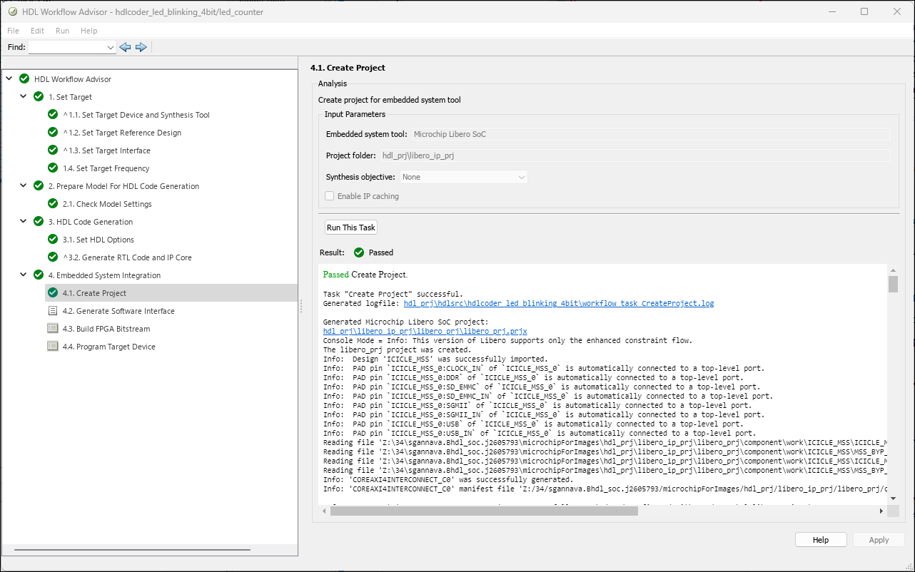
1. To integrate with the Microchip Libero environment, select the Create Project task under Embedded System Integration. Click Run This Task. A Microchip Libero project with the IP Integrator embedded design is generated.
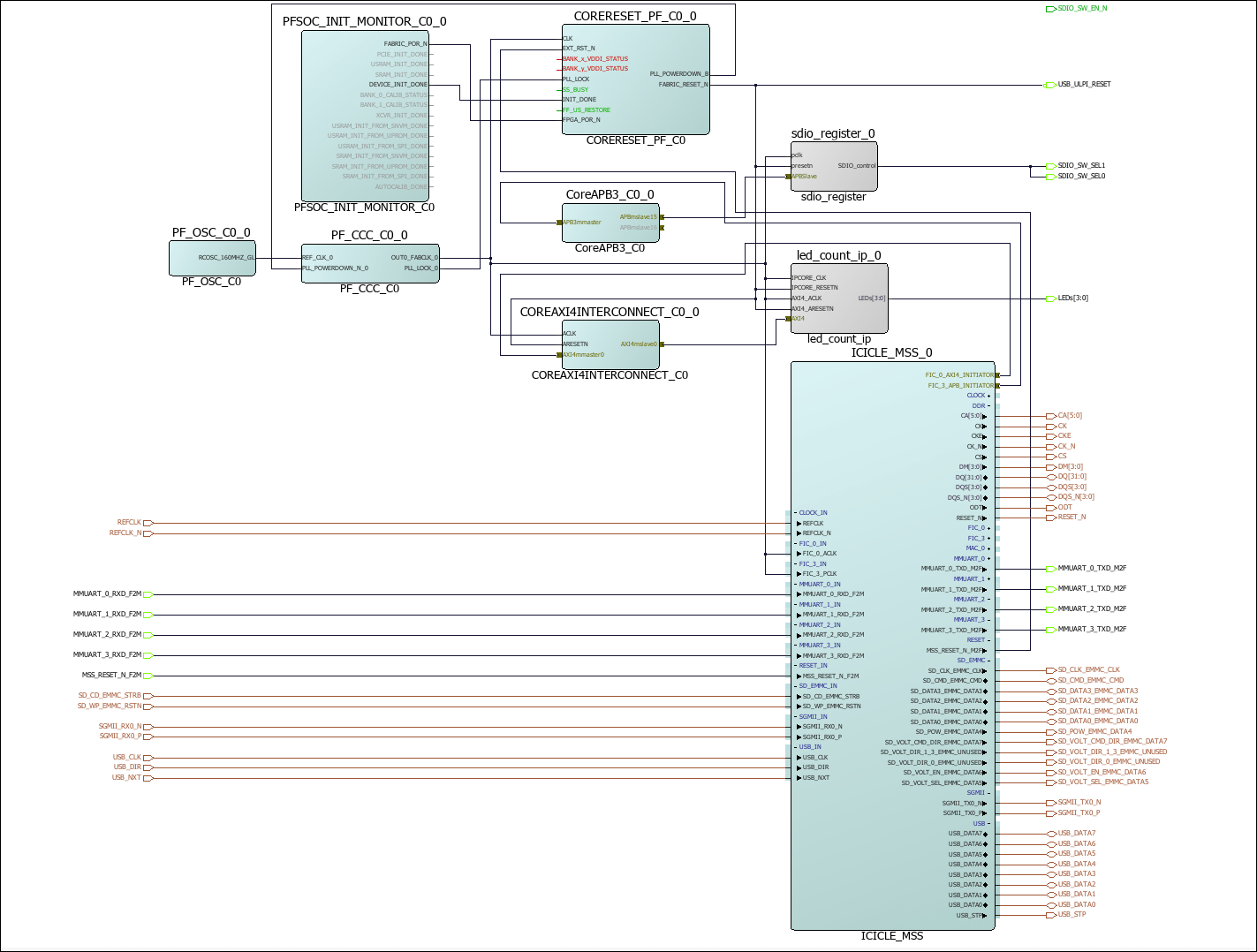
A link to the project is provided in the dialog box. You can optionally open up the project to take a look. From the block diagram in Libero tool, you can see the HDL Coder generated IP core led_count_ip_0 is connected to the Microprocessor Subsystem through the AXI interface.
2. Next, select task 4.2 Generate Software Interface.
In the task 4.2 Generate Software Interface, select Generate host interface script option. The host interface script contains commands that enable you to connect to the target hardware and to write to or read from the generated IP core over the AXI interface.
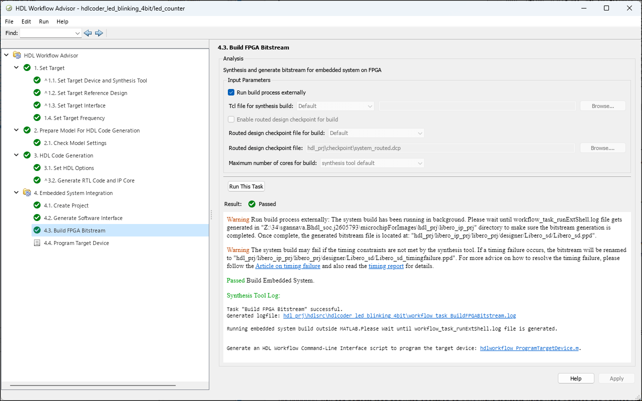
3. Build the FPGA bitstream in the Build FPGA Bitstream task. If you select Run build process externally option then Libero synthesis tool runs in a separate process from MATLAB. You have to wait until workflow_task_runExtShell.log file gets generated in hdl_prj\libero_ip_prj folder.
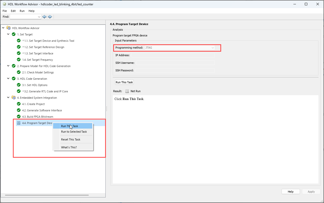
4. After you generates bitstream, select the task 4.4 Program Target Device and click Run This Task to program the PolarFire SoC hardware. Programming method option is set to JTAG to download the FPGA bitstream on the PolarFire SoC board. When you power on the PolarFire SoC board, your design is automatically reloaded on your SoC hardware.
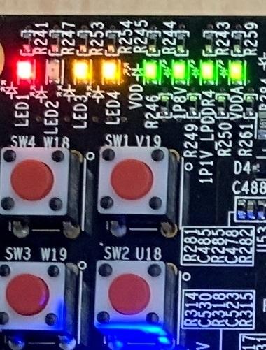
After you program the FPGA hardware, the LED starts blinking on your PolarFire SoC board.
Read Values of the Input Registers
To read the value of input registers, you use register base address with interface mapping address. You can get the register base address from the IP Core Generation report. You can readback of input registers either by using a Devmem command in Linux console or by using MATLAB FPGA prototyping script.
Readback of Input Registers by Using Devmem Command
You can use Devmem command in the Linux console with PuTTy™ or Hyper software. Once you program the bitstream into the target device, open PuTTy or Hyper terminal using serial interface. In the IP core generation report, see Register Address Mapping to get the base address of registers. You can see that register base address is 0x60000000. You can use this base address with address offset to perform read and write operation on registers.
To change the blink frequency of LEDs, run this devmem command on the PuTTY terminal.
devmem2 0x60000100 w 0x05
To change the blink direction of LEDs, run this devmem command on the PuTTY terminal.
devmem2 0x60000104 w 0x01
To readback value of blink direction, run this devmem2 command.
devmem2 0x60000104
The command return value as 0x00000001, which you have written in previous step.
Readback Values of AXI4 Registers by Using MATLAB FPGA IO Prototyping Script
When you select the Generate host interface script option, HDL Coder generates two MATLAB files, gs_hdlcoder_led_blinking_4bit_interface.m and gs_hdlcoder_led_blinking_4bit_setup.m.
gs_hdlcoder_led_blinking_4bit_interface.m- This interface script creates a target object, instantiates the setup script and connects to the target hardware. The script sends read and write commands to the generated HDL IP core.gs_hdlcoder_led_blinking_4bit_setup.m- This setup function adds the register interface. The script also contains DUT port objects that have the port name, direction, data type, and interface mapping information. The script maps the DUT ports to the corresponding interfaces.
To access data from the AXI Register by using the readPort and writePort functions, you can run the host interface scripts or follow these steps:
1. Set up the hardware connection by entering this command in the MATLAB Command Window.
hProcessor = microchipsoc
The microchipsoc function logs in to the hardware over SSH. You can also specify the board's IP address as part of this command.
2. Create a FPGA object by running this command:
hFPGA = fpga(hProcessor)
3. Run the gs_hdlcoder_led_blinking_4bit_setup(hFPGA) setup function with the generated FPGA object as the input argument.This function configures the FPGA object with the same interfaces as the generated IP core.
gs_hdlcoder_led_blinking_4bit_setup(hFPGA)
4. Run the writePort command to change the blinking frequency of LEDs:
writePort(hFPGA, "Blink_frequency", 6)
5. Use the readPort command to read the values from the read back port Read_back.
data_Read_back = readPort(hFPGA, "Read_back")
Summary
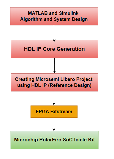
This example shows how the hardware and software co-design workflow helps automate the deployment of your MATLAB and Simulink design to a Microchip PolarFire SoC Icicle Kit. You can explore the best ways to partition and deploy your design by iterating through the workflow.
The following diagram shows high-level picture of the workflow you went through in this example. To learn more about the hardware and software co-design workflow, see Hardware-Software Co-Design Workflow for SoC Platforms.