What Is Signal Integrity?
Signal integrity is the process of maintaining the quality of high-speed digital signals. Signal integrity is a critical measure of the quality of an electrical signal as it travels from a source to its destination. In high-speed digital and analog electronics, ensuring that the intended shape, timing, and power of the signal are preserved guarantees the reliable and accurate transmission of data.
Reflections, noise, electromagnetic interference (EMI), and other issues can severely degrade signal quality. A lack of signal integrity can lead to a cascade of problems, including intermittent faults, data errors, system failures, and, ultimately, costly redesigns and financial losses. From complex printed circuit board (PCB) designs to advanced communication systems, robust signal integrity is the bedrock of dependable performance.
Role of Signal Integrity in System Design
Pre-Layout Analysis for Signal Integrity in High-Speed Designs
One critical step in achieving good signal integrity is performing pre-layout analysis. This type of analysis is typically done during the design phase and aims to identify potential issues and help you make informed decisions that optimize the design for signal integrity.

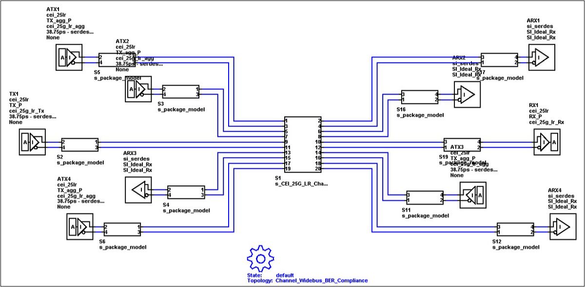
OIF CEI 25G-LR pre-layout schematic built using the Serial Link Designer app in Signal Integrity Toolbox. (See documentation.)
By performing pre-layout analysis, you can spot and resolve potential signal integrity issues early in the design cycle, reducing the risk of costly design revisions and modifications later on. This analysis also helps you optimize the design for signal integrity, resulting in a more robust and reliable design that is compliant with industry standards.
Real-World Applications
Pre-layout PCB signal integrity analysis is especially critical in industries and applications where high-speed, high-reliability communication is essential, such as:
- Data centers, where high-throughput servers rely on clean signal transmission across backplanes and interconnects
- Automotive electronics, where advanced driver-assistance systems (ADAS) and infotainment require robust high-speed communication
- High-speed memory interfaces such as DDR, LPDDR, and GDDR, where timing margins are tight and even minor distortions can cause data corruption
By integrating signal integrity simulation into the early design phase, you can ensure your systems meet performance targets and regulatory standards from the start.
Learn More About Pre-Layout Analysis
Post-Layout Verification for Ensuring PCB Signal Integrity
Post-layout verification involves reviewing the physical implementation of the design, including the actual PCB layout and routing, to ensure that it meets the expected signal integrity performance. The process involves using signal integrity simulation and analysis tools, such as Signal Integrity Toolbox™, to simulate the electrical behavior of the final design and identify any potential issues.

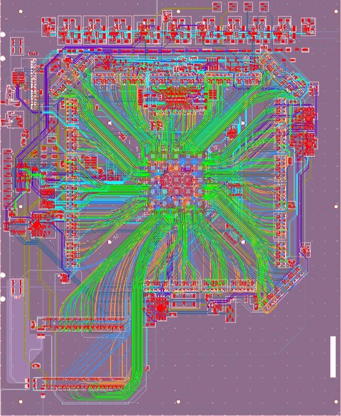
Printed circuit board as shown in the Signal Integrity Viewer app in Signal Integrity Toolbox. (See documentation.)
During post-layout verification, you can perform simulations to calculate the timing, voltage levels, and signal integrity metrics such as jitter, eye height/width, and bit error rate (BER) to validate the design’s performance and ensure it meets industry standards.
If any signal integrity issues are identified, you can make modifications to the layout, routing, or component selection and rerun the simulations until the design meets the expected performance. In some cases, post-layout verification may reveal issues that were not identified during pre-layout analysis, and you must make necessary changes to meet the design requirements.
Real-World Applications
Post-layout verification is vital in industries where performance and compliance are non-negotiable, such as:
- Telecommunications infrastructure, where high-speed serial links must meet stringent signal integrity standards
- Consumer electronics, where compact PCB layouts increase the risk of interference and signal degradation
- Aerospace and defense systems, where reliability under extreme conditions is critical
By integrating post-layout signal integrity simulations into the verification process, you can ensure that your high-speed digital designs are robust, compliant, and ready for production.
Learn More About Post-Layout Verification
Equalization and Channel Modeling for High-Speed Signal Integrity
IBIS-AMI (I/O Buffer Information Specification–Algorithmic Modeling Interface) is a modeling standard used for both pre-layout analysis and post-layout verification of high-speed channels. IBIS-AMI combines the electrical properties of individual components within a signal path to form a complete channel model, enabling you to simulate complex high-speed digital systems with greater accuracy and efficiency.

IBIS-AMI models of a SerDes as shown in Signal Integrity Toolbox (top), the SerDes Designer app (middle), and Simulink (bottom). (See documentation.)
Using IBIS-AMI models in both pre- and post-layout analysis can help you optimize design time, reduce the risk of design errors, and improve the overall signal integrity performance of high-speed digital systems. However, creating accurate and reliable IBIS-AMI models can be a complex and time-consuming process, requiring technical expertise. You can use built-in support in SerDes Toolbox™ for statistical and time-domain simulations, IBIS-AMI parameter management, and automated generation of IBIS-AMI compliant models, which enable you to focus on design optimization and validation.
Real-World Applications
Equalization and channel modeling are critical in systems where high-speed data must travel across complex or lossy media, such as:
- Data center interconnects, where long PCB traces and cables introduce significant signal loss
- High-speed memory interfaces such as DDR, LPDDR, and GDDR, where tight timing margins demand precise signal conditioning
- Automotive Ethernet and infotainment systems, where equalization ensures reliable communication over twisted pair cables
By integrating signal integrity simulation with equalization and channel modeling, you can design systems that meet performance targets even under challenging physical constraints.
Learn More About Equalization and Channel Modeling
Compliance and Standards Verification in Signal Integrity Analysis
In the electronics industry, ensuring compliance with industry standards is a critical part of signal integrity analysis. As data rates increase and protocols become more complex, verifying that a design meets industry specifications is essential for data transmission reliability and product certification.
Using MATLAB® and Simulink®, you can perform automated compliance checks against a wide range of high-speed interface standards, including:
- PCI Express® (PCIe)
- USB 3.x and USB4®
- Optical Internetworking Forum (OIF) and IEEE 802.3 Ethernet
- DDR/LPDDR/GDDR memory interfaces
- Automotive Ethernet and MIPI® standards
These tools enable you to simulate real-world operating conditions, generate eye diagrams, and evaluate jitter, noise margins, and BER to ensure that designs meet the required thresholds. This level of signal integrity simulation helps you identify and resolve issues before hardware testing, reducing the risk of costly redesigns or compliance failures.
Real-World Applications
Compliance verification is especially important in industries where interoperability and certification are mandatory, such as:
- Consumer electronics, where devices must pass USB compliance testing to reach the market
- Automotive systems, where Ethernet and MIPI interfaces must meet strict EMI and timing standards
- Enterprise networking and storage, where PCIe and high-speed memory interfaces must deliver consistent performance under heavy data loads
By integrating compliance verification into the high-speed digital design workflow, you can ensure that your products are not only functional but also standards compliant and ready for global deployment.
Learn More About Compliance and Standards Verification
Signal Integrity Analysis Metrics and Visualizations
In high-speed digital design, signals must remain intact during transmission to achieve good signal integrity performance. Commonly used metrics and visualizations include:
- Voltage margin: The voltage margin measures the difference between the amplitude of the signal and the signal’s noise margin. The voltage margin should be sufficiently high to ensure that the signal can be reliably demodulated at the receiver.
- Timing analysis: This metric involves calculating the signal’s rise and fall times, propagation delay, and jitter. You can use timing analysis to evaluate the design’s timing budget and ensure that the signal transitions within the required timing window.
- Jitter: Jitter is the variation in the signal’s timing over time. Jitter can result from a variety of sources, including signal distortion, crosstalk, power supply noise, and attenuation. You can use jitter histograms and eye diagrams to identify and analyze jitter in high-speed digital systems.
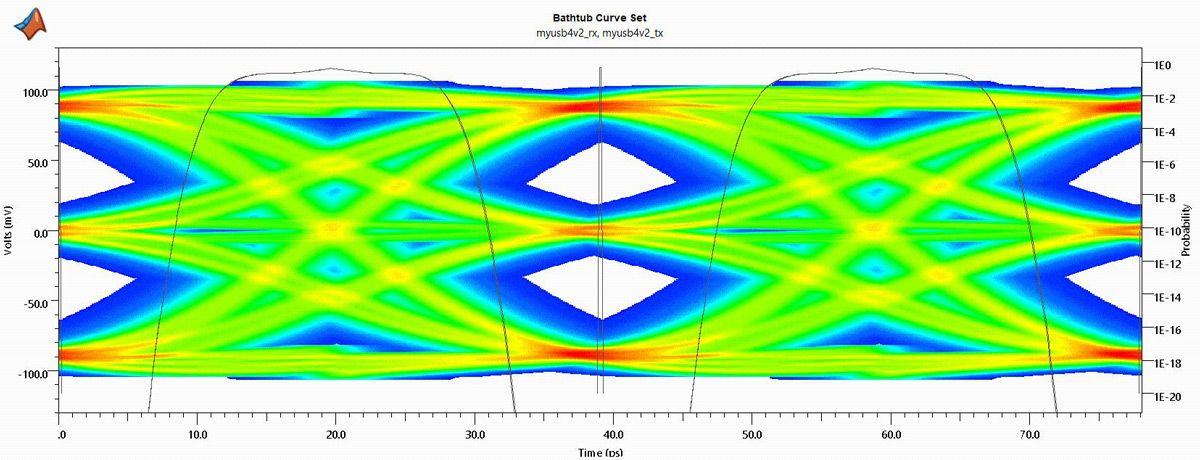
- Eye diagram: Eye diagrams are used to analyze the signal’s performance over time and identify potential signal integrity issues. They involve plotting a graph of the signal’s amplitude against time, usually in the form of a histogram. This visualization technique provides a comprehensive view of the signal’s behavior, including jitter, noise, and timing issues.
- Bit error rate: BER calculates the number of erroneous bits in a data stream. A high BER value indicates poor signal integrity performance. You can use BER to quantify the design’s signal integrity performance then optimize the design to reduce BER.
- Attenuation: Attenuation is a measure of signal loss over distance or time. High levels of attenuation can result in signal distortion and signal failure. You can use attenuation measurements to evaluate the signal’s performance and design transmission lines and circuits to minimize attenuation.
- Crosstalk: Crosstalk occurs when one signal’s electrical field induces noise into an adjacent signal. You can use crosstalk measurements to evaluate the level of interference between channels, calculate the crosstalk coupling coefficient, and identify design methods to reduce the crosstalk level.
- Time-domain reflectometry (TDR): TDR measures the impedance of a transmission line by comparing the signal’s output with the input signal reflected from the end of the line. This technique helps to locate impedance variations and signal integrity issues along transmission lines.
- Channel operating margin (COM): COM quantifies the design’s margin between the signal’s eye and the worst-case impairments. COM helps you evaluate the design’s signal integrity performance and identify areas for improvement.

Example waveform showing thresholds and parameters measured in the Parallel Link Designer app in Signal Integrity Toolbox. (See documentation.)

PAM3 eye diagram created with Signal Integrity Toolbox and shown in the Signal Integrity Viewer app. (See documentation.)
Signal Integrity Analysis with MATLAB and Simulink
To proactively address these challenges, you can use MATLAB and Simulink for signal integrity analysis. By modeling and simulating entire systems, you can detect eye diagram closure, jitter, excessive bit error rates, and other potential issues before physical prototyping. This virtual testing enables you to design and verify equalization techniques, optimize high-speed links, and ensure overall signal quality, saving significant time and resources in the development cycle.
With MATLAB and Simulink products for signal integrity analysis, you can perform:
- Pre-layout analysis in high-speed designs: Identify and resolve potential signal integrity issues early through simulation and modeling before PCB layout begins.
- Post-layout verification: Validate real-world signal behavior and detect layout-induced problems using post-layout PCB signal integrity verification.
- Equalization and channel modeling: Design and simulate equalization strategies to mitigate signal distortion and maintain data integrity across lossy channels.
- Compliance and standards verification: Ensure your design meets industry standards such as PCIe, USB, and DDR through automated compliance testing and simulation.
Signal Integrity Toolbox, SerDes Toolbox, RF PCB Toolbox™, and Mixed-Signal Blockset™ provide features ranging from pre-layout analysis to post-layout verification of a system while producing visualizations such as eye diagrams, waveform plots, frequency spectra, eye contours, and skew budget analysis. These tools provide comprehensive means to prevent issues in data communication systems or high-speed electronics.
Learn More About Capabilities in MATLAB and Simulink
Examples and How To
Software Reference
See also: Signal Integrity Toolbox, SerDes Toolbox, RF PCB Toolbox, RF Toolbox, Mixed-Signal Blockset, mixed-signal systems, IBIS-AMI models, S-parameters, convolution, fast Fourier transform (FFT)
