PCIe6 Transmitter/Receiver IBIS-AMI Model
This example shows how to create IBIS-AMI models for a PCI-Express Generation 6 (PCIe Gen6) transmitter and receiver using the library blocks in SerDes Toolbox™. The IBIS-AMI models generated by this example can be used in Serial Link Designer from Signal Integrity Toolbox™ and conform to the PCIe Gen6 Base-Specification published by the PCI-SIG.
PCIe Gen6 Tx/Rx IBIS-AMI Model Setup in SerDes Designer App
The first part of this example sets up the target transmitter and receiver AMI model architecture using the blocks required for PCIe Gen6 in the SerDes Designer app. The model is then exported to Simulink® for further customization. You can configure the various settings using values from the PCIe Gen6 Base Specification (abbreviated below as "P6BS").
This example uses the SerDes Designer model pcie6_ibis_txrx.mat. Type the following command in the MATLAB® command window to open the model:
>> serdesDesigner('pcie6_ibis_txrx');
![]()
Configuration Setup
Symbol Time is set to 31.25 ps (P6BS Table 8-6), since the maximum allowable PCIe Gen6 data rate is 64 GT/s with PAM4, which equates to a Nyquist frequency of 16GHz (P6BS 4.2.3.1.1).
Target BER is set to
1e-6(P6BS 4.2.1.1).Samples per Symbol is set to 16 (default, not defined by specification).
Modulation is set to PAM4 (P6BS 4.2.1.1.1).
Signaling is set to
Differential.
Transmitter Model Setup
The Tx FFE block is set up for four cursors: two pre-taps, one main tap, and one post-tap. The initial setting is as follows:
Tap Weights is
[0.083 -0.208 0.709 0](P6BS Table 8-2, Preset 7).Note: Specific tap presets can be configured to be selectable options later in this example when the system is exported to Simulink.
The Tx AnalogOut block is configured as follows:
Voltage is 0.8V or 1.0V (P6BS 8.3.6, Table 8-6, [min or max]).
Rise time is 7.5 ps (P6BS 8.4.2.1).
R (output resistance) is
50Ohms (P6BS Table 8-10 note 3).C (capacitance) is
0.1pF (default value, not defined in specification).
Channel Model Setup
Channel loss is set to
24dB (28 dB is maximum loss for Base channel plus CEM card, P6BS 8.4.1.4).Differential impedance is set to
85Ohms (P6BS, 8.4.1.2, Figure 8-28 and 8-29).Target Frequency is set to the Nyquist frequency of
16GHz, which corresponds to 64GT/s with modulation set to PAM4 (P6BS 4.2.1.1.1).
Receiver Model Setup
The Rx AnalogIn block is configured as follows:
R (input resistance) is
50Ohms (P6BS Table 8-10, note 3).C (capacitance) is
0.2pF (default value, not defined in specification).In the Rx CTLE block, you can see the FilterMethod is set to Cascaded to accommodate repeated poles as detailed in the PCIe Gen6 Base Specification (Equation 8-7). The Rx CTLE set up for 11 configurations (0 to 10) and the associated GPZ Matrix matches the Poles and Zeros (P6BS Section 8.4.1.7 and 8.4.1.9 for 64.0 GT/s).
The Rx DFE/CDR block is set up for 16 DFE taps. The limits for each tap have been individually defined according to the PCIe Gen6 specification in section 8.4.1.10. The indicated limits on DFE tap magnitude are only to bound the behavior of a reference receiver.
The conditions used to find taps for this example are as follows (P6BS Section 8.4.1.10):
complies with condition (where the "" brackets indicate absolute value)
Note: This is an example set of cursors, example DFE Tap configuration, given our interpretation of the specification. Equation for 64.0 GT/s DFE tap limits described in section 8.4.1.10.
Reference values only for use in this example for DFE taps d1 through d16 are as follows:
Initial tap weights (V): [0 0 0 0 0 0 0 0 0 0 0 0 0 0 0 0]
Minimum tap value (V): [-0.4 -0.2 -0.125 -0.125 -0.125 -0.125 -0.04 -0.04 -0.04 -0.04 -0.04 -0.04 -0.04 -0.04 -0.04 -0.04]
Maximum tap value (V): [0.4 0.2 0.125 0.125 0.125 0.125 0.04 0.04 0.04 0.04 0.04 0.04 0.04 0.04 0.04 0.04]
Note: You will see how to configure these as a selectable Range after exporting the system to Simulink.
Receiver Model Setup: Find the CTLE GPZ Matrix from the PCIe Gen6 BASE Specification
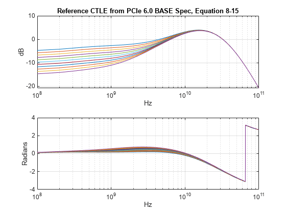
You can see from the loaded model, that the Rx CTLE block is setup for 11 configurations (0 through 10) to accommodate the Gain range of -5 to -15dB for this peaking filter. The code below shows you a method to find a GPZ Matrix for the CTLE block using the transfer equation provided by the PCIe Gen6 Base Specification (Equation 8-15):
% Based on the PCIe Gen6 Base Specification, Equation 8-15:
DCgain = 5:15; %Adc defined as a range from -5 to -15dB in steps of 1dB for 64.0 GT/s Rx Equalization.
ADC = 10.^(-DCgain/20);

z1 = 250e6; %Hz
wz1 = 2*pi*z1;
p1 = 1.30 * z1; %Hz
wp1 = 2*pi*p1;
p2 = 7.7e9; %Hz
wp2 = 2*pi*p2;
p3 = 22.0e9; %Hz
wp3 = 2*pi*p3;
p4 = 28.0e9; %Hz
wp4 = 2*pi*p4;
p5 = 32.0e9; %Hz
wp5 = 2*pi*p5;
p6 = 32.0e9; %Hz
wp6 = 2*pi*p6;

z3 = 7.7e9; %Hz
wz3 = 2*pi*z3;

f = linspace(0,100e9,1001);
w = 2*pi*f;
s = 1j*w;

H = zeros(length(ADC),length(f));

for ii = 1:length(ADC)
    z2(ii) = abs(ADC(ii))*p2;
    wz2(ii) = 2*pi*z2(ii);
    H(ii,:) = ((wp1*wp3*wp4*wp5*wp6)/(wz1*wz3)).*(((s+wz1).*(s+wp2*ADC(ii)).*(s+wz3))./((s+wp1).*(s+wp2).*(s+wp3).*(s+wp4).*(s+wp5).*(s+wp6)));
end

figure(1)
ax1(1) = subplot(211);
semilogx(f,db(H))
grid on
xlabel('Hz')
ylabel('dB')
title('Reference CTLE from PCIe 6.0 BASE Spec, Equation 8-15')
ax1(2) = subplot(212);
semilogx(f,unwrap(angle(H)))
grid on
xlabel('Hz')
ylabel('Radians')
linkaxes(ax1,'x')
%Define gpz matrix [G,P1,Z1,P2,Z2,P3,0,P4]:
gpz = zeros(length(ADC),8);
gpz(:,1) = -DCgain;
gpz(:,2) = -p1;
gpz(:,3) = -z1; %z1
gpz(:,4) = -p2;
gpz(:,5) = -z2;
gpz(:,6) = -p3;
%Note: Zero, pad column 7 with zeros since there are 2 more poles than
%zeros.
gpz(:,8) = -p4;
Note: you can transfer Gain-Pole-Zero data contained in the workspace variable gpz into your model with the following steps:
1) Open gpz and copy paste data into SerDes Designer.
2) After running script, simply type gpz in SerDes Designer.
Plot Statistical Eye Diagram and BER
You can use various plot types in SerDes Designer to visualize the output and performance of the PCIe Gen6 system. You can test the system by configuring the following settings:
Rx CTLE Mode set to
adapt.DFECDR Mode set to
adapt.DFECDR 2x tap weights set to
disabled.DFECDR PhaseDetector set to
BangBang.
Next, select the BER plot from the "ADD Plots" menu in the toolstrip and observe the Statistical Eye Diagram is displayed along with BER.
![]()
Receiver Model for Captive Device: Plot Statistical-Mode Results
Note that a minimum compliance for the Receiver which may be used to evaluate Eye Diagrams is defined as follows (P6BS, Table 8-16):
Voltage Minimum: 6.0 mVpp
Timing Minimum: 0.1 UI (3.125ps)
Note: You can find various performance metrics by selecting Report from the Add Plots tab in the toolstrip.
Jitter Setup for Transmitter and Receiver
You can click on the Tx/Rx Jitter button on the toolstrip to view the Jitter Parameters tab. The Report tab you have open presently will enable you to observe how much the Statistical Eye Diagram and BER plot change as you enable or disable the various jitter types in the Jitter Parameters tab.
Tx Jitter Parameters
You can verify the Jitter parameters are set correctly by referencing the PCIe Gen6 Base specification, table 8-6, "Data Rate Dependent Transmitter Parameters."
Note: These parameters will export as type "Float" with format "Value." After exporting to Simulink, you can change these to format "Range" using the IBIS-AMI Manager.
**Tx DCD Jitter Value (**Ttx-upw-tj from Table 8-6 in the PCIe Gen6 Base Spec)
Confirm value is
4.0e-12(Note: this is the maximum allowed per specification).Confirm units is set to seconds.
Tx Rj **Jitter Value (**Ttx-rj from table 8-6)
Confirm value is
0.42e-12(Note: this is the maximum allowed per specification).Confirm units is set to seconds.
Tx Dj **Jitter Value (**Ttx-upw-djdd from Table 8-6)
Confirm value is 1.25e
-12(Note: this is the maximum allowed per specification).Confirm units is set to seconds.
Rx Jitter Parameters
Rx DCD Jitter Values
Confirm value is
0.Confirm units is set to seconds.
Rx Rj **Jitter Values (**Trx-st-rj from Table 8-11)
Confirm value is
0.25e-12(Note: this is the maximum allowed per specification).Confirm units is set to seconds.
Rx Dj Jitter Values
Confirm value is
0.Confirm units is set to seconds.
To visualize the effect of various jitter types, you can drag the tab for Report across to the bottom of the BER plot and the dialog box will automatically provide a split-pane to display both tabs as follows:
![]()
You may observe that the Statistical Eye and BER plot is nearly closed, but this is expected. There are many reasons this could occur, some of which include:
Jitter parameters from the specification are maximum allowed values and there is no expectation they would each be maximum at the same time in a real world system.
The DFE cursors in this example are provided for reference only to satisfy the mathematical bounds provided for 64.0GT/s DFE (P6BS 8.4.1.10), and a real-world set of cursors may be defined to optimize for certain types of jitter reduction.
Before exporting to Simulink, re-enable Tx_DCD, Tx_Rj, Tx_Dj, and Rx_DCD, Rx_Rj, Rx_Dj. Enabling these jitter parameters automatically includes them in this SerDes System when exporting to Simulink. Later you will see how to change these to ranges and set each one to 0 as a default value.
Note: After exporting to Simulink, you can also edit their Type, Usage, Format, and Value using the IBIS-AMI manager.
Export SerDes System to Simulink
Click on the Export button in the toolstrip to export the above configuration to Simulink for further customization and generation of the IBIS-AMI model files.
PCIe Gen6 Tx/Rx IBIS-AMI Model Setup in Simulink
The second part of this example takes the SerDes system exported by the SerDes Designer app and customizes it as required for PCIe Gen6 in Simulink. The following steps show how to configure the details of the system to prepare for exporting IBIS-AMI models.
Review Simulink Model Setup
The SerDes System imported into Simulink consists of Configuration, Stimulus, Tx, Analog Channel and Rx blocks. All the settings from the SerDes Designer app have been transferred to the Simulink model. Save the model and review each block setup.
![]()
You can confirm settings are carried over from the SerDes Designer app by double clicking the Configuration block and the Analog Channel block. This opens the Block Parameters dialog box so you can review their values.
You can double click the Tx block and the Rx block to look inside each of their subsystems which are inherited from the SerDes Designer app.
Setup Stimulus
Before running a SerDes system in Simulink, you can configure the Stimulus block for Number of symbols, Waveform creation method, and other metrics as follows:
Set the Number of symbols to 75000.
Set the Waveform creation method to Serial PRBS. This will create a repeating pattern of Pseudo-Random Symbols as a stimulus which can exercise the link in a way that maximizes inter-symbol interference (ISI) during GetWave (Time Domain) simulation.
Leave the other values set to defaults and click OK to close the dialog box.
![]()
Set Ignore Bits
Next, open the IBIS-AMI Manager from the Configuration Block. You can set the “bits to ignore” for the Tx to 4, because the FFE has 4 taps. Also, you can set “bits to ignore” for the Rx to 50000 (default is 1000), which should be a sufficient value for the DFECDR to converge during time domain simulation, given its number of taps.
Note: Ignore Bits set in this dialog box must always be fewer than Number of Symbols set in the Stimulus block in order to show GetWave (Time Domain) waveforms (this also applies to any EDA tool running IBIS-AMI models).
![]()
Update Tx Jitter Parameters
If you forgot to enable them in SerDes designer, you can still add the Tx Jitter parameters by clicking on the AMI - Tx Tab. Then click on the Reserved Parameters button. Check the boxes to enable the following parameters to appear in the .ami file:
Tx_DCD
Tx_Dj
Tx_Rj
![]()
Then you will see the parameters displayed in the Reserved Parameters listing:
![]()
For each jitter parameter, you can set the appropriate IBIS variable metrics. For example, in the case of for the Jitter Parameters as follows.
Set Tx DCD Jitter Values (Ttx-upw-tj from Table 8-6)
Select Tx_DCD, then click the Edit... button to bring up the Add/Edit AMI Parameter dialog box.
Verify the Type is
Float.Change the Format to
Range.Set the Current Value to
0.Set the Typ value to
0.Set the Min value to
0.Set the Max value to 4.0
e-12.Click OK to save the changes.
![]()
Set Tx Dj Jitter Values (Ttx-upw-djdd from Table 8-6)
Select Tx_Dj, then click the Edit... button to bring up the Add/Edit AMI Parameter dialog box.
Follow the steps for Tx_DCD, above.
Set the Max value to 0.26
e-12.Click OK to save the changes.
Set Tx Rj Jitter Values (Ttx-rj from table 8-6)
Select Tx_Rj, then click the Edit... button to bring up the Add/Edit AMI Parameter dialog box.
Follow the steps for Tx_DCD, above.
Set the Max value to
0.45e-12.Click OK to save the changes.
Update Receiver AMI Parameters
Open the AMI-Rx tab in the SerDes IBIS/AMI manager dialog box. Following the format of a typical AMI file, the reserved parameters are listed first followed by the model specific parameters.
Update Rx Jitter Parameters
Select the Rx_DCD, Rx_Dj and Rx_Rj as follows:
![]()
They are now shown in the Reserve Parameters of the AMI - Rx tab:
![]()
Set Rx DCD Jitter Values
Select Rx_DCD, then click the Edit... button to bring up the Add/Edit AMI Parameter dialog box.
Change the Type to
Float.Change the Format to
Range.Set the Current Value to
0.Set the Typ value to
0.Set the Min value to
0.Set the Max value to
0.Note: you are setting these values to zero so that the IBIS keyword for Rx_DCD appears in the .ami file in the event that a user or model enhancement occurs later, this metric can be updated in any EDA tool rather than having to re-generate the IBIS-AMI models.
Click OK to save the changes.
Set Rx Rj Jitter Values (Trx-st-rj from Table 8-9)
Select Rx_Rj, then click the Edit... button to bring up the Add/Edit AMI Parameter dialog box.
Follow the steps for Rx_DCD, above, setting all values to 0.
Set the Max value to
0.25e-12.Click OK to save the changes.
Set Rx Dj Jitter Values
Select Rx_Dj, then click the Edit... button to bring up the Add/Edit AMI Parameter dialog box.
Follow the steps for Rx_DCD, above.
Click OK to save the changes.
Note: you can close the IBIS AMI Manager for the next section. You can revisit this dialog box to export IBIS-AMI models later.
Review Tx FFE Block
Inside the Tx subsystem, double click the FFE block to open the FFE Block Parameters dialog box.
Verify that the current value of Mode is set to
Fixedand click OK to close the dialog box.
![]()
Review Rx CTLE Block
Inside the Rx subsystem, double click the CTLE block to open the Block Parameters dialog box.
Gain pole zero data is carried over from the SerDes Designer app. This gain pole zero data applies the transfer function of the behavioral CTLE given by the PCIe Gen6 Base Specification.
Verify that the CTLE Mode is set to
Adapt, which means an optimization algorithm built into the CTLE system object selects the optimal configuration at run time.
![]()
Review Rx DFECDR Block
Inside the Rx subsystem, double click the DFECDR block to open the DFECDR Block Parameters dialog box.
Expand the IBIS-AMI parameters to show the list of parameters to be included in the IBIS-AMI model.
You can see that the DFE tap values are carried over from the SerDes Designer app:
![]()
Next, click on the CDR tab. You can see how to configure the CDR block below.
Configure Rx CDR Block
Simulink supports Time Domain simulation, so you can configure the CDR block to perform clock recovery based on UI and other parameters depending on your particular implementation.
Because the CDR block represents a digital implementation, it can only approximate the behavior given for the continuous-function of a behavioral CDR for 64.0GT/s (P6BS section 8.4.1.5), you can make adjustments as necessary but for this example we will proceed with CDR defaults and set the sensitivity to a fraction of a valid eye diagram height (V).
You can set the CDR parameters as follows:
Phase Offset is set to 0 UI (default)
Reference is set to 0 ppm (default)
Early/late count threshold is set to 16
Step is set to 0.0078 (default)
Sensitivity is set to 0.0001V (e.g. set to approximately 1/10 fraction of minimum eye height if 6mV, P6BS Table 8-11)
Note: You will need to click on Refresh Init to promote this change to the system.
![]()
Generate PCIe Gen6 Tx/Rx IBIS-AMI Model
The final part of this example generates IBIS-AMI compliant model files using SerDes Toolbox.
Open the Block Parameter dialog box for the Configuration block and click on the Open SerDes IBIS/AMI Manager button. In the IBIS tab inside the SerDes IBIS/AMI manager dialog box, the analog model values are converted to standard IBIS parameters that can be used by any industry standard simulator. In the AMI-Tx and AMI-Rx tabs, the reserved parameters are listed first followed by the model specific parameters following the format of a typical AMI file.
Update Transmitter AMI Parameters
Open the AMI-Tx tab in the SerDes IBIS/AMI manager dialog box. Following the format of a typical AMI file, the reserved parameters are listed first followed by the model specific parameters.
To select PCIe Gen6 Tx Preset Ratio coefficient values Q0 through Q10 (as provided in P6BS Table 8-2), you have to set the TX FFE tap values by creating a new Tx AMI parameter and implement an algorithm in the Init customer specific code section.
Click on the FFE parameter listed under the Model_Specific section, then click on the button “Add Parameter.” Then configure the options in the dialog box as follows:
Parent Node: FFE (default)
Parameter name: ConfigSelect
Description: PCIe Gen6 Tx FFE tap weights configuration
Usage: In
Type: Integer
Format: List
Default: -1 (-1 is used to select “user defined” taps, it is not a Preset from the specification)
List values: [-1 0 1 2 3 4 5 6 7 8 9 10]
List_Tip values: ["User Defined" "Q0" "Q1" "Q2" "Q3" "Q4" "Q5" "Q6" "Q7" "Q8" "Q9" "Q10"]
Current value: User Defined
![]()
Note: When you directly specify the preset coefficients, you change the format of the TapWeights and specify the exact value to use for each preset. Only these presets will be allowed, and all three taps must be set to the same preset to get the correct values.
Create Common Function to Call from Init and from GetWave
There are two simulations modes, Init (Linear Time-Invariant system, Statistical or Convolution processing) and GetWave (Time Domain bit-by-bit processing). Both modes can reference the same function to select Tx FFE presets as shown below (and provided with this example as file TxFFEPreset_PCIe_G6.m).
% Derived from PCIe-Gen6 Specification, Tx FFE Presets, Table 8-2.
function TapWeightsOut = TxFFEPreset_PCIe_G6(``TapWeightsIn``, ConfigSelect``)
switch ConfigSelect
case -1 % User defined tap weights
TapWeightsOut = TapWeightsIn;
case 0 % Preset Configuration: Q0
TapWeightsOut = [0 0 1 0];
case 1 % Preset Configuration: Q1
TapWeightsOut = [0 -0.083 0.917 0];
case 2 % Preset Configuration: Q2
TapWeightsOut = [0 -0.167 0.833 0];
case 3 % Preset Configuration: Q3
TapWeightsOut = [0 0 0.917 -0.083];
case 4 % Preset Configuration: Q4
TapWeightsOut = [0 0 0.833 -0.167];
case 5 % Preset Configuration: Q5
TapWeightsOut = [0.042 -0.208 0.75 0];
case 6 % Preset Configuration: Q6
TapWeightsOut = [0.042 -0.125 0.708 -0.125];
case 7 % Preset Configuration: Q7
TapWeightsOut = [0.083 -0.208 0.709 0];
case 8 % Preset Configuration: Q8
TapWeightsOut = [0.083 -0.25 0.667 0];
case 9 % Preset Configuration: Q9
TapWeightsOut = [0.083 -0.25 0.625 -0.042];
case 10 % Preset Configuration: Q10
TapWeightsOut = [0 0 1 0];
otherwise
TapWeightsOut = TapWeightsIn;
end
end
Modify Init (Statistical Mode) to Select Presets for Transmitter Preshoot Tap, Main Tap, and De-emphasis Tap
In this section, you will see how to utilize the newly added ConfigSelect parameter in the Transmitter Subsystem to select Transmitter FFE tap Presets.
Note: If a ConfigSelect value of -1 is used, then the user-defined Tx tap values are passed through to the FFE datapath block from the User via the EDA tool.
To begin, within the Tx subsystem, double-click on the Init block, then click the Refresh Init button to open the Init function to update Init with the new ConfigSelect parameter added earlier. Next, click the Show Init button to open the Init function in an editor window.
This will automatically display the Initialize MATLAB function which provides the impulse response processing of the SerDes system block (IBIS-AMI Init).
To add the custom ConfigSelect control code, scroll down the Custom User Code area, comment out the FFEParameter.ConfigSelect lines, then enter the following code, as you see here:
%% BEGIN: Custom user code area (retained when 'Refresh Init' button is pressed)
%FFEParameter.ConfigSelect; % User added AMI parameter from SerDes IBIS-AMI Manager
FFEInit.TapWeights = TxFFEPreset_PCIe_G6(FFEParameter.TapWeights,FFEParameter.ConfigSelect);
% END: Custom user code area (retained when 'Refresh Init' button is pressed)
Note: Data in this section will not get over-written when the Refresh Init button is clicked:
To test the new parameter, you will need to run simulations and see that the FFE taps are changing (in Init only at this point). Another option is to press Ctrl-D to compile the model but not run simulation. This will check for errors/warnings (note: there may be 1 warning).
![]()
This corresponds to PCIe Gen6 Tx FFE Configuration Q7: PreShoot 2 = 0.083, PreShoot 1 = -0.208, Main = 0.709 and Post = 0.
Modify GetWave (Time Domain Mode) to Select Transmitter Presets for Pre-shoot Tap, Main Tap, and De-emphasis Tap
To modify GetWave (Time Domain) to enable the same sort of selector, add a new MATLAB function that operates in the same manner as the Initialize function.
Inside the Tx subsystem, type Ctrl-U to look under the mask of the FFE block.
![]()
You can see that a new constant block has been added called FFEParameter.ConfigSelect. This is created automatically by the IBIS-AMI Manager when a new AMI Parameter is added. Next, you can follow these steps to re-configure the selection of tap weight presets for time domain (GetWave) simulation:
Add a MATLAB Function block to the canvas from the Simulink/User-Defined library.
Double-click the MATLAB Function block and replace the template code with the following:
function TapWeightsOut = TxFFEConfig(TapWeightsIn, ConfigSelect)
% Call external file TxFFEPreset
TapWeightsOut = TxFFEPreset_PCIe_G6(TapWeightsIn, ConfigSelect);
end
Re-wire the FFE sub-system so that the FFEParameter.TapWeights and FFEParameter.ConfigSelect constant blocks connect to the inputs of the newly defined TxFFEconfig MATLAB function block. The TapWeightsOut signal from the TxFFEconfig block connects to the TapWeights port of the FFE block.
![]()
Run the SerDes System Model in Simulink
You can now run the model to simulate the SerDes System. Two plots are generated, the first is a live Time Domain (GetWave) eye diagram that is updated as the model is running.
![]()
The second plot contains views of the statistical (Init) results and persistent time domain (GetWave) results, similar to what is available in the SerDes Designer app.
![]()
You may notice that the eye height can differ between Statistical and Time Domain. There are many possible reasons for larger eye diagram openings in Time Domain: one example could be use of encoding in the Stimulus to control ISI, another example could be active behavior of a DFE, etc. You can explore the system to visualize its performance while changing various characteristics such as setting CTLE to fixed, etc.
Export IBIS-AMI Models
Open the Export tab in the SerDes IBIS/AMI manager dialog box, and re-verify the following settings:
Verify the Tx model name is pcie_g6
_tx.Verify the Rx model name is pcie_g6
_rx.Note that the Tx and Rx corner percentage is set to
10. This will scale the min/max analog model corner values by +/-10%.Verify that Dual model is selected for both the Tx and the Rx AMI Model Settings. This will create model executables that support both statistical (Init) and time domain (GetWave) analysis.
Set the Tx model Bits to ignore value to 4 since there are four taps in the Tx FFE.
Set the Rx model Bits to ignore value to
50000to allow sufficient time for the Rx DFE taps to settle during time domain simulations.Set Models to export as Both Tx and Rx so that all the files are selected to be generated (IBIS file, AMI files and DLL files).
Set the IBIS file name to be pcie_g6.ibs.
![]()
Click the Export button to generate models in the Target directory.
Test Generated IBIS-AMI Models
The PCIe Gen 6 transmitter and receiver IBIS-AMI models are now complete and ready to be utilized in any industry standard EDA tool capable of IBIS-AMI simulation.
See Also
FFE | CTLE | DFECDR | SerDes Designer
Topics
- Managing AMI Parameters
- Customizing SerDes Toolbox Datapath Control Signals
- PCIe-5 Compliance Kit (Signal Integrity Toolbox)
- PCIe5 Transmitter/Receiver IBIS-AMI Model
- PCIe4 Transmitter/Receiver IBIS-AMI Model