Model Configuration Parameters for Texas Instruments C2000 Processors
To configure hardware parameters for Texas Instruments® C2000™ processors:
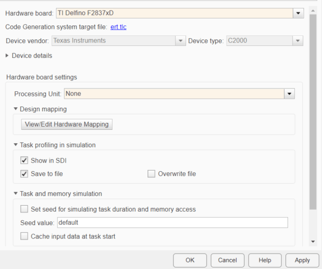
In the Simulink® Editor, select Modeling > Model Settings.
In the Configuration Parameter dialog box, click Hardware Implementation.

Set the Hardware board parameter to your C2000 processors.
The parameter values under Hardware board settings are automatically populated to their default values.
You can optionally adjust these parameters for your particular use case.
Note
When selecting the processing unit, choose the central processing unit (CPU) or control law accelerator (CLA) or CortexM4 onto which to deploy the model block in the model. The default values varies based on the processor selected.
Click Apply.
Note
In the Hardware board drop-down list, some processors have multiple options. Select the generic option for controlCARDs and custom boards, and select the LaunchPad option for LaunchPads. For example, select TI Delfino F2837xS as the generic option, and select TI Delfino F28377S Launchpad as the LaunchPad option. Based on your selection, the default values for clock settings, pin selection, and memory mapping change.
Hardware Board Settings
| Parameter | Description | Default Value |
|---|---|---|
| Processing Unit | Processor or CLA for model block in the MCU model. | None |
Task Profiling in Simulation
| Parameter | Description | Default Value |
|---|---|---|
| Show in SDI (SoC Blockset) | Show the task execution data collected in simulation in the Simulation Data Inspector application. | on |
| Save to file (SoC Blockset) | Save the task execution data to a file. | on |
| Overwrite file (SoC Blockset) | Overwrite the last task execution data file. | off |
Task Profiling on Processor
| Parameter | Description | Default Value |
|---|---|---|
| Show in SDI (SoC Blockset) | Show the task execution data collected on hardware in the Simulation Data Inspector application. | off |
| Save to file (SoC Blockset) | Save the task execution data to a file. | off |
| Overwrite file (SoC Blockset) | Overwrite the last task execution data file. | off |
| Instrumentation (SoC Blockset) | Choose to perform code instrumentation or Kernel instrumentation. | Code |
| Profiling duration (SoC Blockset) | Choose whether to perform Kernel profiling for an unlimited or limited time duration. | Unlimited |
Simulation Settings
| Parameter | Description | Default Value |
|---|---|---|
| Set random number generator seed (SoC Blockset) | Set the random number generator seed. | off |
| Seed Value (SoC Blockset) | Specify the seed value for the simulation of task duration deviation. |
|
| Cache input data at task start (SoC Blockset) | Cache the input data at the start of a task. |
|
Hardware Board Settings
For each hardware board you select, you can configure the board parameters according to your requirements.
Scheduler Options
| Parameter | Description | Default Value |
|---|---|---|
| Base rate trigger | Set the static priority of the base rate task in the operating system. |
|
Build Options
| Parameter | Description | Default Value |
|---|---|---|
Define how Embedded Coder® responds when you build your model. |
| |
Select to compile the generated code and driver source codes in parallel order for faster build and deployment speed. | off | |
Select your device from the selected processor family. | ||
| Enable TMU | Enables support for Trigonometric Math Unit (TMU). |
|
Specify if the application loads to the flash memory. |
| |
Indicates that the custom linker command file must be used during the build action. |
| |
The path to the memory description file required during linking. | ||
The Code Composer Studio™ file required for downloading the application on the hardware. | ||
| Select to access ePWM Registers | ||
Enable DMA to peripheral frame 1 (ePWM, HRPWM, eCAP, eQEP, DAC,CMPSS, and SDFM) instead of CLA | Select to enable the DMA to access peripheral frame 1 | |
Enable DMA to peripheral frame 2 (SPI and McBSP) instead of CLA | Select to enable the DMA to access peripheral frame 2 | |
| Enables use of optimized floating point math functions from C28x FPU fastRTS library | enabled | |
Remap ePWMs for DMA access (Requires silicon revision A and above) | Select to remap ePWMs registers for DMA access | |
| Enable this option to configure LSRAM memory for CLA program or data. |
| |
| Select the maximum LSRAM size that is available for CLA program in KiloWords. | ||
| Select the maximum LSRAM size that is available allowed for CLA data in KiloWords. | ||
| Displays the remaining available LSRAM size for CPU in KiloWords. | ||
Use data type replacement to override precision of ‘double’ in generated code | Enable Use data type replacement to override precision of ‘double’ in generated code parameter to override precision of ‘double’ in generated code. |
|
| Select the number of bits for double. | 32 | |
| Generates html report with the list of double datatype usages in model. | ||
| Enable the parameter to load C28x IQmath library blocks from flash memory and execute them from RAM. | on |
Clocking
| Parameter | Description | Default Value |
|---|---|---|
| Specify the desired CPU clock frequency (CLKIN). | ||
| Use the internal zero pin oscillator on the CPU. |
| |
| Oscillator clock (OSCCLK) frequency in MHz | Oscillator frequency used in the processor. | |
| PLL values in PLLCR, DIVSEL, and Achievable SYSCLKOUT in MHz are automatically calculated based on the CPU clock entered on the board. | ||
| If you select Auto set PLL based on OSCCLK and CPU clock, the auto-calculated control register value matches the specified CPU clock value, based on the oscillator clock frequency. | ||
40 | ||
PLL output divider (ODIV) /System PLL output divider (SYSPLLMULT_ODIV) | Calculates SYSCLKOUT = ((OSCCLK×SYSPLLMULT)/ODIV)/SYSDIVSEL. | 1 |
| If you select Auto set PLL based on OSCCLK and CPU clock, the auto-calculated control register value matches the specified CPU clock value, based on the oscillator clock frequency. | 2 | |
System PLL raw clock value in MHz: PLLRAWCLK = ((OSCCLK*SYSPLLMULT_IMULT)/SYSPLLMULT_ODIV) | 400 | |
1 | ||
| The auto-calculated feedback value that matches the Desired C28x CPU clock in MHz value, based on the values of OSCCLK, PLLCR, and DIVSEL. | ||
Set the 'Achievable SYSCLKOUT in MHz = (OSCCLK*SYSPLLMULT)/SYSDIVSEL' value calculated in CPU1 | Available only for CPU2 of dual C28x core processors. Value of this parameter must be same as the value of the parameter Achievable SYSCLKOUT in MHz = (OSCCLK*PLLCR)/DIVSEL (auto calculated). | |
Select the 'Low-Speed Peripheral Clock Prescaler (LSPCLK)' option used in CPU1 | Available only for CPU2 of dual C28x core processors. Value of this parameter must be same as the value of the parameter Low-Speed Peripheral Clock Prescaler (LSPCLK) specified in CPU1. | |
| Prescaler value used to calculate LSPCLK based on SYSCLKOUT. | ||
| The LSPCLK value calculated using the SYSCLKOUT and LSPCLK Prescaler values. | ||
| Prescaler value used to calculate HSPCLK based on SYSCLKOUT. | ||
| The HSPCLK value calculated using the SYSCLKOUT and HSPCLK Prescaler values. | ||
The multiplication factor value of PLL clock. | 12 | |
The value is calculated based on Multiplication factor for PLL#CLK (PLL#MULT) and OSCCLK frequency. | 120 | |
| Prescaler value used to calculate ASYSCLK based on SYSCLKOUT. | ||
| The ASYSCLK value calculated using the SYSCLKOUT and ASYSCLK Prescaler values. | ||
| Specify the connectivity manager clock frequency (in MHz) supplied to ARM Cortex-M core. | 100 | |
| Select the auxiliary PLL clock source. | Internal oscillator | |
| Specify the auxiliary PLL output divider. | 10 | |
Auto set Auxiliary PLL based on AUXOSCCLK and desired CM clock | on | |
| Specify the auxiliary PLL output divider. | 1 | |
| Specify the auxiliary PLL multiplier. | 40 | |
| Specify the auxiliary PLL reference divider. | 1 | |
| Specify the auxiliary PLL raw clock value in MHz. | 400 | |
| Select the clock source for ARM Cortex-M core. | System PLL | |
| Select the divider for the ARM Cortex-M core clock. | 4 | |
| The calculated value of the clock frequency (in MHz) supplied to ARM Cortex-M core. | 100 | |
| Select the Ethernet clock divider (ETHDIV) based on your desired Ethernet clock in MHz. | 4 | |
Ethernet clock in MHz :(AUXPLLRAWCLK or SYSPLLRAWCLK) / ETHDIV | Ethernet clock in MHz is calculated as (AUXPLLRAWCLK or SYSPLLRAWCLK) / (ETHDIV + 1), where ETHDIV is the value set in the EMAC clock divider register. | 100 |
Ethernet clock source for Connectivity Manager (Arm Cortex-M4) | The Connectivity Manager on Arm Cortex-M4 based TI C2000 MCUs, typically derived from the AUXPLLRAWCLK (Auxiliary PLL output) or SYSPLLRAWCLK (System PLL output), selectable via the EMACCLKSEL register. | SYSPLLRAWCLK |
ADC_x
| Parameter | Description | Default Value |
|---|---|---|
| The CPU core that controls the ADC module. | Auto | |
| The ADCCLK divider for the c2802x, c2803x, c2806x, F28M3x, F2807x, or F2837x processor. | SYSCLKOUT/5.0 | |
| ADC clock frequency in MHz | The clock frequency for ADC, which is auto generated based on the value you select in ADC clock prescaler (ADCCLK). | 40 |
| Enable or disable overlap of sample and conversion. | ||
| The HSPCLK is divided by ADCLKPS (a 4-bit value) as the first step in deriving the core clock speed of the ADC. |
| |
| After dividing the HSPCLK speed by the ADC clock prescaler (ADCLKPS) value, divides the result by 2. | 1 | |
ADC Module clock (ADCCLK = HSPCLK/ADCLKPS×2)/(CPS+1)) in MHz | The ADC module clock, which indicates the ADC operating clock speed. | |
| Determine the width of the sampling or acquisition period. A higher value indicates a wider sampling period. |
| |
Acquisition window size ((ACQ_PS+1)/ADCCLK) in micro seconds/channel | Determine the duration for which the sampling switch is closed. | |
| Specify the offset value. | ||
| Allows using a 2.048 V external voltage reference. | ||
| Allows using an external voltage reference. | ||
| When the ADC generates an end of conversion (EOC) signal, an ADCINT# interrupt is generated. The interrupt indicates whether the previous interrupt flag has been acknowledged. | ||
| The 280x ADC supports offset correction using a 9-bit value that it adds or subtracts before the results are available in the ADC result registers. |
| |
| When you disable the Use external reference 2.048V or External reference option, the ADC logic uses a fixed 0–3.3 V input range, and VREFHI and VREFLO are disabled. To interpret the ADC input as a ratiometric signal, select the External reference option. Then, set values for the high-voltage reference (VREFHI) and the low voltage reference (VREFLO). | ||
| Set the time when the ADC sets ADCINTFLG ADCINTx relative to the SOC and EOC pulses. | ||
| Enable SOC high priority mode. |
| |
| The pin to which the ADC sends the XINT2SOC pulse. | ||
| The GPIO pin from which ADC receives the ADCEXTSOC pulse. | GPIO# | |
| Indicates the input of X-BAR for ADC external SOC. | Input# |
COMP
| Parameter | Description | Default Value |
|---|---|---|
| Comparator x (COMPx) pin assignment | Assign COMP pin to a GPIO pin. |
DAC
| Parameter | Description | Default Value |
|---|---|---|
| DACx reference voltage | Select the reference voltage for the DAC channel A, B, or C. | ADC reference voltage (VREFHIA/VREFHIB) |
| DACx synchronization signal | Select the synchronization signal to load the value from the writable shadow register into the active register. | SYSCLK |
CAN_x
| Parameter | Description | Default Value |
|---|---|---|
| The clock for the enhanced CAN module. | 200 | |
| The clock for the enhanced CAN module. | ||
Baud rate prescaler (BRP: 2 to 256)/Baud rate prescaler (BRP: 1 to 1024) | Scale the bit rate using this value. | 20 |
| Set the value of time segment 1. This value, with TSEG2 and Baud rate prescaler, determines the length of a bit on the CAN bus. | ||
| Set the value of time segment 2. This value, with TSEG1 and Baud rate prescaler, determines the length of a bit on the CAN bus. | ||
Baud rate (CAN Module Clock/BRP/(TSEG1 + TSEG2 +1)) in bits/sec | CAN module communication speed represented in bits/second. | |
| Set the message resynchronization triggering. | ||
| Set the synchronization jump width, which determines how many units of TQ a bit can be shortened or lengthened by when resynchronizing. | ||
| Number of samples used by the CAN module to determine the CAN bus level. | ||
| Enable time stamping and usage of Mailbox Numbers 16 through 31 in the C2000 CAN blocks. | ||
If you set this parameter to True, the CAN module
goes to loopback mode. The loopback mode sends a dummy acknowledge message
back. |
| |
| Assign the CAN transmit pin to use with the CAN_B module. | ||
| Assign the CAN receive pin to use with the CAN_B module. |
eCAP
| Parameter | Description | Default Value |
|---|---|---|
| ECAPx capture pin assignment | Indicates the GPIO pin used for eCAP in capture mode. | GPIO# |
| ECAPx Input X-BAR | Select input X-BAR for ECAP | INPUT# |
| ECAPx APWM pin assignment | The GPIO pin to which output of the eCAP in APWM mode is sent. | GPIO# |
| Output X-BAR | Indicates which Output X-BAR is used for the selected ECAP# APWM pin assignment parameter. | # |
| eCAPxSYNCIN source selection | Indicates the SYNC source select register for the ePWM SYNCOUT, eCAP SYNCOUT, INPUTXBAR and EtherCATSYNC. | The default eCAPxSYNCIN source selection value varies based on
the processor selected. |
ePWM
| Parameter | Description | Default Value |
|---|---|---|
| Select the ePWM clock divider. | SYSCLKOUT/1 | |
Select the 'EPWM clock divider (EPWMCLKDIV)' option used for CPU1 | Available only for CPU2 of dual C28x core processors. Its value must be the same as the value of the parameter EPWM clock divider (EPWMCLKDIV) selected in CPU1. | |
| Indicates the trip-zone input X-BAR. | INPUT# | |
| Indicates the GPIO pin to the trip-zone input x (TZx). | None | |
| Select the TRIP Multiplexer(MUX). | Disable all | |
| Indicates the inputs selected for each MUX so far. | XXXXXXXXXXX | |
Select the input to the Multiplexer selected in TRIP# MUX
select. | X:Disable | |
| Option to reset the MUX inputs selected. | ||
| Inverts the TRIP output signal. | off | |
| Indicates the SYNCI input X-BAR. | INPUT# | |
| Indicates the GPIO pin used for the ePWM external sync pulse input (SYNCI). | None | |
| Assign the ePWM external sync pulse output (SYNCO) to a GPIO pin. | ||
| Select the external SYNCOUT source for ePWM | Default value varies based on the processor
selected | |
| Select the EPWMxSYNCIN Source Select Register (synchronization input pulse) for the ePWM | Default value varies based on the processor
selected | |
Assign the GPIO pin to the PWM#x module. | GPIO# | |
| Assign the ePWM trip-zone input to a GPIO pin. | ||
| Assign the ePWM sync pulse input (SYNCI) to a GPIO pin. | ||
| Assign the Digital Compare A high trip input to a GPIO pin. | ||
| Assign the Digital Compare A low trip input to a GPIO pin. |
I2C
| Parameter | Description | Default Value |
|---|---|---|
Configure the I2C module as
controller or
peripheral. | ||
In peripheral
mode, determines the addressing format of the I2C
controller and sets the I2C module to the same
mode. | ||
In
| ||
In
| ||
In
| ||
Display the frequency the I2C module uses internally. To set this value, change the Module clock prescaler. | ||
I2C controller clock frequency (Module Clock Freq/(ICCL+ICCH+10)) in Hz | Display the controller clock frequency. | |
In
| ||
In
| ||
In
| ||
Select a GPIO pin as an I2C data bidirectional port. | ||
Select a GPIO pin as an I2C clock bidirectional port. | ||
This parameter corresponds to bit 5 (TXFFIENA) of the I2C Transmit FIFO Register (I2CFFTX). | ||
This parameter corresponds to bits 4–0 (TXFFIL4-0) of the I2C transmit FIFO register (I2CFFTX). | ||
This parameter corresponds to bit 5 (RXFFIENA) of the I2C receive FIFO register (I2CFFRX). | ||
This parameter corresponds to bit 4–0 (RXFFIL4-0) of the I2C receive FIFO register (I2CFFRX). | ||
Select this parameter to configure the five basic I2C interrupt request parameters in the interrupt enable register (I2CIER). | ||
Enable the addressed-as-peripheral interrupt bit. | ||
Enable the stop condition detected interrupt bit. | ||
Enable the register-access-ready interrupt bit. | ||
Enable the no acknowledgment interrupt bit. | ||
Enable the arbitration-lost interrupt bit. |
SCI_x
| Parameter | Description | Default Value |
|---|---|---|
Enable the loopback function for self-test and diagnostics. | ||
| The type of suspension to use while debugging your program with Code Composer Studio. | ||
Specify the number of stop bits transmitted. | ||
| The type of parity to use. | ||
Length in bits of each transmitted or received character. |
| |
Specify the desired baud rate. | ||
| Scale the SCI baud rate using this value. | ||
The closest achievable baud rate, calculated based on LSPCLK and BRR. | ||
| Select the mode for transmitting and receiving data. | ||
Posts interrupt when available data in transmit FIFO is less than or equal to interrupt level. | off | |
Level for triggering SCI transmit interrupt. | 1 | |
Posts interrupt when available data in receive FIFO is greater than or equal to interrupt level. | off | |
Level for triggering SCI receive interrupt. | 1 | |
Select an option to match the endianness of the data being moved. | ||
Assign the SCI transmit pin to use with the SCI module. | ||
Assign the SCI receive pin to use with the SCI module. |
SPI_x
| Parameter | Description | Default Value |
|---|---|---|
Set to | ||
Specify the desired baud rate. | ||
| The value used to calculate the baud rate. | ||
Closest achievable baud rate (LSPCLK/(SPIBRR+1)) in bits/sec | The closest achievable baud rate, calculated based on LSPCLK and SPIBRR. | |
| The type of suspension to use while debugging your program with Code Composer Studio. | ||
| Enable the loopback function for self-test and diagnostics. |
| |
| Enables SPI communication over three pins instead of the normal four pins. |
| |
Enable SPI transmit interrupt operation. |
| |
Set level for transmit FIFO interrupt. |
| |
Enable SPI receive interrupt operation. |
| |
Enable high speed SPI mode for supported pins. | ||
Set level for receive FIFO interrupt. | ||
FIFO transmit delay (in processor clock cycles) to pause between data transmissions. | ||
Assign the SPI (SIMO) to a GPIO pin. | ||
Assign the SPI value (SOMI) to a GPIO pin. | ||
Assign the CLK pin to a GPIO pin. | ||
Assign the SPI value (STE) to a GPIO pin. |
eQEP
| Parameter | Description | Default Value |
|---|---|---|
Assign eQEP pin to a GPIO pin. |
Watchdog
| Parameter | Description | Default Value |
|---|---|---|
Enable the watchdog timer module. | ||
Set the watchdog timer period relative to OSCCLK/512. | ||
Display the timer period in seconds. This value automatically updates when you change the Counter clock parameter. | ||
Configure the watchdog to reset the processor or generate an interrupt when the software fails to reset the watchdog counter. |
GPIO
| Parameter | Description | Default Value |
|---|---|---|
Use the GPIO pins for digital input or output by connecting to one of the three peripheral I/O ports. |
DMA_ch#
| Parameter | Description | Default Value |
|---|---|---|
Enable to edit the configuration of a specific DMA channel. | ||
Select the size of the data bit transfer. | ||
Select the peripheral interrupt that triggers a DMA burst for the specified channel. | ||
| Specify the number of bursts before returning the current source address pointer to the Source Begin Address value. | ||
| Specify the number of bursts before returning the current destination address pointer to the Destination Begin Address value. | ||
| Set the starting address for the current source address pointer. | ||
| Set the starting address for the current destination address pointer. | ||
| Specify the number of 16-bit words in a burst, from 1 to 32. | ||
Specify the number of bursts in a transfer, from 1 to 65536. | ||
| Increment or decrement the current address pointer by this number of 16-bit words before the next burst. | ||
| Increment or decrement the current address pointer by this number of 16-bit words before the next burst. | ||
| Increment or decrement the current address pointer by this number of 16-bit words before the next transfer. | ||
| Increment or decrement the current address pointer by this number of 16-bit words before the next transfer. | ||
| Increment or decrement the SRC_BEG_ADDR address pointer by this number of 16-bit words when a wrap event occurs. | ||
| Increment or decrement the DST_BEG_ADDR address pointer by this number of 16-bit words when a wrap event occurs. | ||
Enable this parameter to have the DMA channel send an interrupt to the CPU through the Peripheral Interrupt Expansion (PIE) at the beginning or end of a data transfer. | ||
Enable this parameter to have the DMA channel complete an entire transfer in response to an interrupt event trigger. | ||
| Enable this parameter to reset the DMA wrap counter when the Interrupt source is set to SEQ1INT and sends the ADCSYNC signal to the DMA wrap counter. | ||
Select this parameter to leave the DMA channel enabled upon completing a transfer. The channel waits for the next interrupt event trigger. | ||
Enabling this parameter resets the destination wrap counter (DST_WRAP_COUNT) when Sync enable is enabled and the DMA module receives the SEQ1INT interrupt/ADCSYNC signal. | ||
Enable this option when DMA channel 1 is configured to handle high-bandwidth data, such as ADC data, and the other DMA channels are configured to handle lower-priority data. | ||
Enable this parameter to have the DMA channel send an interrupt to the CPU through the PIE if the DMA module receives a peripheral interrupt while a previous interrupt from the same peripheral is waiting to be serviced. |
EMIF#
| Parameter | Description | Default Value |
|---|---|---|
| EMIF clock divider (EMIF1CLKDIV) | Clock divider for clock frequency generation. | SYSCLKOUT/2 |
| Enable CS0 for Synchronous memory | Chip select (CS0) to interface with the SDRAM. | off |
| Enable CS# for Asynchronous memory | Chip select (CS2/CS3/CS4) to interface with the asynchronous RAM. | off |
| SDRAM Column address bits | Value of the column address bits or the required page size of the connected SDRAM. | 8 |
| Number of internal SDRAM banks | Number of memory banks inside the connected SDRAM. | 3 |
| SDRAM data bus width in bits | Data bus width of the connected SDRAM. | 16 |
| Refresh to active command delay cycles (T_RFC) | Minimum number of EM#CLK cycles from the refresh or load mode command to the refresh or activate command in the connected SDRAM. | 3 |
| Row precharge to Active command delay cycles (T_RP) | Minimum number of EM#CLK cycles required from the row precharge command to the activate or refresh command in the connected SDRAM. | 1 |
| Active to read or write command delay cycles (T_RCD) | Minimum number of EM#CLK cycles from the activate command to the read or write command in the connected SDRAM. | 2 |
| Last write to row precharge command delay cycles (T_WR) | Minimum number of EM#CLK cycles from the last write transfer or last data in command to the row precharge command in the connected SDRAM. | 1 |
| Active to precharge command delay cycles (T_RAS) | Minimum number of EM#CLK cycles from the activate command to the row precharge command in the connected SDRAM. | 4 |
| Active to active command delay cycles (T_RC) | Minimum number of EM#CLK cycles from an activate command to the next activate command in the same bank in the connected SDRAM. | 6 |
| Active one bank to active another bank command delay cycles (T_RRD) | Minimum number of EM#CLK cycles from an activate command in one bank to an activate command in a different bank in the connected SDRAM. | 1 |
| Self-refresh exit to other command delay cycles (T_XSR) | Minimum number of EM#CLK cycles from the self refresh exit command to any other command in the connected SDRAM. | 7 |
| SDRAM refresh period (tRefreshPeriod) in ms | Defines the rate at which the connected SDRAM refreshes. | 64 |
| SDRAM CAS Latency | CAS latency required to access the connected SDRAM. | 3 |
| Asynchronous mode | Asynchronous mode for the connected asynchronous memory. | Normal |
| Asynchronous data bus width in bits | Data bus width of the connected asynchronous memory. | 16 |
| Read strobe setup cycles (R_SETUP) | Number of EM#CLK cycles from the EMIF chip select to the pin enable for asynchronous memory assert. | 15 |
| Read strobe duration cycles (R_STROBE) | Number of EM#CLK cycles during which the pin enable for the asynchronous memory is held active. | 64 |
| Read strobe hold cycles (R_HOLD) | Number of EM#CLK cycles during which the EMIF chip select is held active after pin enable for the asynchronous memory is deasserted. | 7 |
| Write strobe setup cycles (W_SETUP) | Number of EM#CLK cycles from the EMIF chip select to the write enable for the asynchronous memory assert. | 15 |
| Write strobe duration cycles (W_STROBE) | Number of EM#CLK cycles during which the write enable for the asynchronous memory is held active. | 63 |
| Write strobe hold cycles (W_HOLD) | Number of EM#CLK cycles during which the EMIF chip select is held active after write enable for the asynchronous memory is deasserted. | 7 |
| Turn around cycles (TA) | Number of EM#CLK cycles between the end of one asynchronous memory access and the start of another asynchronous memory access. | 3 |
| Enable extended wait mode | Enable the extended wait option for the asynchronous memory. | off |
| Maximum extended wait cycles for Asynchronous memory (MAX_EXT_WAIT) [0–255] | EMIF waits for (MAX_EXT_WAIT+1) * 16 clock cycles before the asynchronous cycle is terminated. | 128 |
| Pin polarity of extended wait | Make EMIF wait if the pin is low or high. | High |
| Enable wait rise interrupt | Get an interrupt based on the detection of a rising edge on the EM#WAIT pin. | off |
| Enable timeout interrupt | Get an interrupt when the EM#WAIT pin does not become inactive within the number of cycles defined in Maximum extended wait cycles for Asynchronous memory (MAX_EXT_WAIT) [0–255]. | off |
| Enable line trap interrupt | Get an interrupt when there is an invalid cache line size or illegal memory access. | off |
LIN
| Parameter | Description | Default Value |
|---|---|---|
Display the frequency of the LIN module clock in MHz. | ||
| Enable LIN loopback testing. | ||
| Use this option to configure how the LIN state machine behaves while you debug the program using an emulator. |
| |
| Use this option to configure parity checking. |
| |
Set the number of data bytes in the response field, from 1–8 bytes. |
| |
| To set the LIN baud manually, enter a prescaler value from 0–16777215. |
| |
| To set the LIN baud manually, enter a fractional divider value from 0–15. |
| |
| Display the baud rate. | ||
Enable or disable the LIN module from using the ID-field bits ID4 and ID5 for length control. |
| |
Set the endianness of the LIN message data bytes. |
| |
| Set the width for data swap. | ||
Map the LINTX output to a specific GPIO pin. |
| |
Map the LINRX input to a specific GPIO pin. |
| |
| Set the LIN module as a controller or a peripheral. |
| |
Select the type of mask filtering comparison the LIN module performs. |
| |
If you set ID filtering as |
| |
If you set ID filtering to ID
peripheral task byte, use this
option to set the ID-peripheralTask BYTE. |
| |
| Select the checksum type. |
| |
| When you select this check box, the LIN node uses transmit and receive buffers instead of just one register. | Selected | |
This option is displayed when you set LIN
mode to
| Not selected | |
If you enable this option, the peripheral node generates interrupts when it detects irregularities in the synch field. |
| |
If you enable this option, the LIN module generates an interrupt if it does not receive a complete response from the controller node within a timeout period. |
| |
When enabled, the peripheralnode generates an interrupt when it sends three wakeup signals to the controller node and does not receive a header in response. |
| |
When enabled, the peripheral node generates an interrupt when it sends a wakeup signal to the controller node and does not receive a header in response. |
| |
When enabled, the peripheral node generates an interrupt after 4 seconds of inactivity on the LIN bus. |
| |
The LIN peripheral mode generates a wakeup interrupt based on a request or condition. |
|
External Interrupt
| Parameter | Description | Default Value |
|---|---|---|
| Indicates the input X-BAR for external interrupt. | Input# | |
The GPIO pin for external interrupt. | 0 | |
Set the polarity for external interrupt. | Falling edge |
External Mode
| Parameter | Description | Default Value |
|---|---|---|
Select the type of communication interface to run your model in external mode. |
| |
Select the serial communication interface module. |
| |
Select the COM port used by the target hardware. | ||
| Select the interface through which the host computer communicates to target hardware for signal monitoring and parameter tuning. |
| |
| Select the CAN module to be used with external mode |
| |
| Select the FIFO# for the receive read source of MCAN module to be used with external mode. This parameter is enabled only for MCAN peripheral. |
| |
Automatically configure or use existing standard/extended filter number for XCP receive | Configure a filter in the MCAN module to work with XCP over MCAN external mode, or specify an unused filter number, which the system will configure at runtime for external mode. This parameter is enabled only for MCAN peripheral. | 0 |
| Enter the CAN ID Command for the CAN module. |
| |
| Enter the CAN ID Response for the CAN module. |
| |
| Enter the CAN vendor for the CAN module. |
| |
| Enter the device for the CAN module. |
| |
| Enter the CAN channel number for the CAN module. |
| |
| Select to use extended ID. |
| |
| Enter the Rx mailbox number for the CAN module. |
| |
| Enter the Tx mailbox number for the CAN module. |
| |
Select to view the external mode execution progress and updates in the Diagnostic Viewer or in the MATLAB® command window. |
| |
Select to automatically set the number of bytes to preallocate for the buffer in the hardware during simulation. |
| |
Specify a value for maximum number of contiguous samples parameter. |
| |
Select to log data inside ISR at ISR trigger rate |
|
Execution Profiling
| Parameter | Description | Default Value |
|---|---|---|
Enter the number of profiling samples to collect. |
SD Card Logging
| Parameter | Description | Default Value |
|---|---|---|
Enables the MAT-file logging for SD card. | off | |
Select the desired interface on which the SD card is connected to hardware board. | ||
Select the desired option for the SPI interface used by the SD card. | Maximum achievable supported by the inserted SD
Card |
CMPSS
| Parameter | Description | Default Value |
|---|---|---|
Configure the comparator subsystem (CMPSS). | off | |
Configure the COMPH or COMPL module. | off | |
Reload condition for RAMP reference value. | Immediate (RAMPMAXREFA) | |
Invert comparator output. | off | |
Enable latch clear by EPWMSYNCPER event. | off | |
Configure the digital filter for COMP#. | off | |
Set the sample clock prescale for digital filter of COMP#. | 0 | |
Set the sample window size for digital filter of COMP#. | 0 | |
Set the threshold sample window size for digital filter of COMP#. | 0 | |
Select the comparator output type source for COMP#. | Asynchronous output (ASYNCH) | |
Select the comparator output type source for COMP#. | Asynchronous output (ASYNCH) | |
Select the DAC reference voltage for CMPSS. | Internal reference voltage (VDDA) | |
Select the reload condition for DAC value. | System clock (SYSCLK) | |
Select the EPWM peripheral synchronization event. | EPWM1SYNCPER | |
Select the EPWM for blanking window | EPWM1BLANK | |
Set the amount of hysteresis on the comparator inputs. | 0 |
SDFM#
| Parameter | Description | Default Value |
|---|---|---|
Configure the filter channel for the SDFM module. | off | |
Select the data pin for the GPIO configuration. | GPIO# | |
Select the clock pin for the GPIO configuration. | GPIO# | |
Select the modulator clock mode. | Same as the modulator data rate (MOD_0) | |
Select the comparator filter type. | Sinc1 | |
Specify the comparator OSR value. | 0 | |
Specify the comparator higher threshold value to detect an over-value condition. | 0 | |
Specify the comparator lower threshold value to detect an under-value condition. | 0 | |
Specify the comparator higher threshold value to detect over-value condition. | 0 | |
Select the data filter type. | Sinc1 | |
Specify the data OSR value. | 0 | |
Specify the FIFO value for the data filter. | 0 | |
Enable to reset the data filter by external PWM compare output. | off | |
Select the ePWM module for synchronization. | PWM#SOCA | |
Select the comparator event (CEVT#) interrupt. | Disable | |
Enable threshold crossing event detection. | off | |
Enable the interrupt for modulator clock failure. | off | |
Enable the interrupt for new data acknowledgment. | off | |
Enable to detect an over-value condition. | off | |
Enable to detect an under-value condition. | off | |
Select to synchronize the data input to a filter with the PLL clock. | off | |
Select to synchronize the clock input to a filter with the PLL clock. | off |
PIL
| Parameter | Description | Default Value |
|---|---|---|
Select the type of communication interface to run your model. |
| |
Select the serial communication interface module. |
| |
Select the COM port used by the target hardware. |
Analog subsystem
| Parameter | Description | Default Value |
|---|---|---|
| Allows using an external voltage reference. | off | |
| High voltage reference. | 3.3 |
Overrun detection
| Parameter | Description | Default Value |
|---|---|---|
| Enable to notify when task overrun occurs. | off | |
| Enable to select GPIO action. | on | |
| Specify the GPIO number of a digital output. | 34 | |
| Select the GPIO mode. | Set | |
| Select the additional option to notify when task overrun occurs. | None | |
| Specify the PIE number for the interrupt to trigger on overrun. | 1 | |
| Specify the CPU number for the interrupt to trigger on overrun. | 1 | |
| Specify the name of the C function to call on overrun. | C2000_OverunFunction |
INPUT X-BAR
| Parameter | Description | Default Value |
|---|---|---|
| Specify the GPIO pin for input X-BAR. | None |
OUTPUT X-BAR
| Parameter | Description | Default Value |
|---|---|---|
| Select the output multiplexer(MUX). | Disable all | |
Select the input to the MUX selected for OUTPUT# MUX
select. | X:Disable | |
| Indicates the input signal selected for each output MUX. | XXXXXXXXXXXXXXXXXXXXXXX | |
| Option to reset the MUX inputs selected. | ||
| Select the GPIO pin for the output X-BAR MUX signals. | GPIO# | |
| Enables the output latch to drive the respective output X-BAR. | off | |
| Inverts the output X-BAR signal. | off |
CLB X-BAR
| Parameter | Description | Default Value |
|---|---|---|
| Select the MUX to map the signal to AUXSIG# MUX. | Disable all | |
Select the input to the MUX selected for AUXSIG# MUX
select. | X:Disable | |
| Indicates the input signal selected for each AUXSIG MUX. | XXXXXXXXXXXXXXXXXXXXXXX | |
| Option to reset the MUX inputs selected. | ||
| Inverts the CLB X-BAR signal or Inverts the AUXSIG# signal. | off |
CLB
| Parameter | Description | Default Value |
|---|---|---|
| Select this option to enable the CLB tile. | off | |
| Specify the tile name. This tile name will be used to generate the required function declaration and calling the function for CLB tile configuration file (clb_config.c and clb_config.h) generated using CLB tool. The tile names entered here should be an exact match with the tile name set in CLB tool to generate the file. | TILE# | |
| Configure the signal source type for the IN# mux. The type of signal can be global inputs, local inputs and GPREG. | Global inputs | |
| Configure the peripheral signal as input to the CLB tile. | ePWM#A | |
| Configure the type of input filtering for the signal type Global inputs and Local inputs. This option will be disabled for GPREG as it is not applicable. | No filtering | |
| Configure the synchronization option (SYNC) for the Global inputs and Local inputs IN# mux selection only. This option is not applicable for GPREG type and will be disabled for the same. | off | |
| Option to enable routing the CLB output signal to the peripheral instead of the default peripheral signal. Each CLB output signal passes through an external multiplexer that intersects a specific peripheral signal. If the options in this parameter is enabled it will route the CLB output for the specific peripheral instead of the original peripheral signal. | | |
| Provide the paths for the CLB configuration header file clb_config.h generated using CLB tool. This file holds the required function declarations and headers used to configure the CLB tile. | clb_config.h | |
| Provide the paths for the CLB configuration source file clb_config.c generated using CLB tool. This file holds the required function definitions used to configure the CLB tile. | clb_config.c | |
| Click this button to browse the path for the file selection. | ||
| Click this button to open the existing file for editing in MATLAB editor. |
HRCAP Model Configuration
| Parameter | Description | Default Value |
|---|---|---|
Select the GPIO pin for the respective HRCAP module. | GPIO# |
MCAN
| Parameter | Description | Default Value |
|---|---|---|
| Select the CAN type. Classic CAN or CAN-FD. | CAN-FD | |
MCAN module clock frequency (=connectivity manager (ARM Cortex-M) clock)in MHz | Displays the MCAN module clock frequency in MHz. | 100 |
| Displays the MCAN bit clock frequency in MHz. | 25 | |
| Nominal bit rate prescaler. The value by which the oscillator frequency is divided for generating the bit time quanta. | 1 | |
| Nominal time segment before sample point. | 22 | |
| Nominal time segment after sample point. | 2 | |
Closest achievable nominal baud rate (MCAN bit clock/NBRP/(NTSEG1+NTSEG2)) in bits/sec | Closest achievable nominal MCAN baud rate in bits/sec. | 1000000 |
| Nominal Resynchronization Jump Width (NSJW). | 1 | |
| Enables bit rate switching between nominal bit rate and data bit rate. | off | |
| Data Bit Rate Prescaler (DBRP). The value by which the oscillator frequency is divided for generating the bit time quanta. | 1 | |
| Data time segment before sample point (DTSEG1). | 22 | |
| Data time segment after sample point (DTSEG2). | 2 | |
Data baud rate (MCAN bit clock/DBRP/(DTSEG1+DTSEG2)) in bits/sec | Closest achievable MCAN data baud rate calculated based on data parameters and given formula. | 1000000 |
| Data resynchronization jump width (DSJW). | 1 | |
| Select the operating mode for MCAN. | Normal | |
| Select a GPIO pin for the MCAN data transmission. | GPIO 31 | |
| Select a GPIO pin for the MCAN data reception. | GPIO 30 | |
| Select the mode of transmission. | FIFO | |
| Enable blocking mode for FIFO 0 data reception. | off | |
| Enable blocking mode for FIFO 1 data reception. | off | |
| Enable this parameter to update standard and extended filter IDs. | off | |
| Rejects all remote frames with 11-bit standard IDs when enabled else the remote frames will be filtered as per the settings from Configure standard filter elements. | off | |
| Rejects all remote frames with 29-bit extended IDs when enabled else the remote frames will be filtered as per the settings from Configure extended filter. | off | |
| Defines how received messages with 11-bit standard IDs that do not match any element from Configure standard filter elements are treated. | Accept in Rx FIFO 0 | |
| Defines how received messages with 29-bit extended IDs that do not match any element from Configure extended filter are treated. | Accept in Rx FIFO 0 | |
| Enable this parameter to update the standard 11bit ID filter elements parameters. | off | |
| Select the standard message ID filter elements. | 0 | |
| Select the standard filter element configuration. | Disable filter element | |
Filter # type (filter type will be ignored if filter configuration is stored into Rx buffer) | Select the standard filter type. | Classic ID and mask filter (ID1 = filter, ID2 =
mask) |
| Specify the standard Filter ID 1. | 0 | |
| Specify the standard Filter ID 2. | 0 | |
| Enable to update the extended filter elements. | off | |
| Select the extended message ID filter elements. | 0 | |
| Select extended filter element configuration. | Disable filter element | |
Filter # type (filter type will be ignored if filter configuration is stored into Rx buffer) | Select the extended filter type. | Classic ID and mask filter (ID1 = filter, ID2 =
mask) |
| Specify the first ID of extended ID filter element. | 0 | |
| Specify the second ID of extended ID filter element. | 0 | |
Display configured extended and standard filters elements in command window | Click on Display configured extended and standard filters elements in command window button to view the configured standard and extended filter elements in MATLAB command window. | |
| Click Reset standard filters configurations to reset the configured standard filter configurations. | ||
| Click Reset extended filters configurations to reset the configured extended filter configurations. | ||
| Select to configure the memory and its parameters. | off | |
| Select the maximum data size of CAN FD message in transmit FIFO. | 64 | |
| Select the maximum data size of CAN FD message in receive FIFO 0. | 64 | |
| Select the maximum data size of CAN FD message in receive FIFO 1. | 64 | |
| Select the maximum data size of CAN FD message in receive buffer. | 64 | |
| Select the number of elements (data + header CAN FD message) in transmit FIFO/Queue. | 32 | |
| Select the number of elements (data + header CAN FD message) in receive FIFO 0. | Auto allocate | |
| Select the number of elements (data + header CAN FD message) in receive FIFO 1. | Auto allocate | |
| Click Validate memory button to validate all the memory configurations. | ||
| Select this option to display receive interrupt sources for configuration. | off | |
| Select this option to display buffer interrupt sources for configuration. | off | |
| Select the dedicated interrupt line for receive buffer message. | Disable | |
| Select the dedicated interrupt line for high priority message. | Disable | |
| Select this option to display receive FIFO 0 interrupt sources for configuration. | off | |
| Select the interrupt line for receive FIFO 0 new message. | Disable | |
| Select the interrupt line for receive FIFO 0 full. | Disable | |
| Select the interrupt line for receive FIFO 0 message lost. | Disable | |
| Select the interrupt line for receive FIFO 0 watermark. | Disable | |
| Select this option to display receive FIFO 1 interrupt sources for configuration. | off | |
| Select the interrupt line for receive FIFO 1 new message. | Disable | |
| Select the interrupt line for receive FIFO 1 full. | Disable | |
| Select the interrupt line for receive FIFO 1 message lost. | Disable | |
| Select the interrupt line for receive FIFO 1 watermark. | Disable | |
| Select this option to display transmit interrupt sources for configuration. | off | |
| Enable to configure the transmit FIFO interrupt sources. | off | |
| Select the transmission interrupt line for transfer complete. | Disable | |
| Select the transmission interrupt line for transfer cancellation finish. | Disable | |
| Select the transmission interrupt line for TX FIFO empty. | Disable | |
| Select this option to display transmit event FIFO interrupt sources for configuration. | off | |
| Select the transmission interrupt line for TX event FIFO new entry. | Disable | |
| Select the transmission interrupt line for TX event FIFO element lost. | Disable | |
| Select the transmission interrupt line for TX event FIFO full. | Disable | |
| Select the transmission interrupt line for TX event FIFO watermark. | Disable | |
| Select this option to display other interrupt sources for configuration. | off | |
| Select the interrupt line for timestamp wraparound interrupt. | Disable | |
| Select the interrupt line for timeout occurred interrupt. | Disable | |
| Select the interrupt line for error logging overflow interrupt. | Disable | |
| Select the interrupt line for warning status interrupt. | Disable | |
| Select the interrupt line for watchdog event interrupt. | Disable | |
| Select the interrupt line for data protocol error interrupt. | Disable | |
| Select the interrupt line for message RAM access failure interrupt. | Disable | |
| Select the interrupt line for bit error uncorrected interrupt. | Disable | |
| Select the interrupt line for error passive status interrupt. | Disable | |
| Select the interrupt line for bus off status interrupt. | Disable | |
| Select the interrupt line for arbitration protocol error interrupt. | Disable | |
| Select the interrupt line for reserved address access interrupt. | Disable |
For more information on selecting a hardware board and general configuration settings, see Hardware Implementation Pane.