UCIe 2.0 Transmitter/Receiver IBIS-AMI Models
This example shows how to create IBIS-AMI models for Universal Chiplet Interconnect Express (UCIe) Revision 2.0, transmitter and receiver for clock and data, using the library blocks in SerDes Toolbox. The IBIS-AMI models generated by this example utilize IBIS Clock Forwarding functionality which can be simulated in Parallel Link Designer from Signal Integrity Toolbox and conform to the UCIe specification.
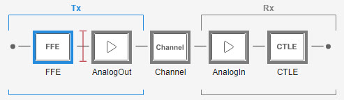
Create Tx and Rx Models for Single-Ended Data and Differential Clock Signals
Parts 1 and 2 of this example will show how to generate single-ended data transmitter and receiver models for a UCIe 2.0 system starting with the SerDes Designer app and then exporting to Simulink® for further customization. You will configure the various settings using values from the UCIe specification (section references provided in-line) in both the SerDes Designer app and in Simulink. These models utilize Rx termination and target an operating speed of 32GT/s using a Standard package.
Parts 2 and 3 will repeat this process for differential clock transmitter and receiver models. These models also target an operating speed of 32GT/s using a Standard package.
This example follows the Universal Chiplet Interconnect Express Specification, Revision 2.0, Version 1.0.
Part 1: Setup Tx and Rx Models for Single-Ended Data in SerDes Designer
Load the system model for the UCIe 2.0 data signals by typing the following command in the MATLAB® command window to open the SerDes Designer model ucie_txrx_data_se.mat:
>> serdesDesigner('ucie_txrx_data_se')
Configuration Setup
Symbol Time is set to
31.25ps representing a data rate of 32 GT/s with NRZ modulation, which equates to a Nyquist frequency of 16GHz.Samples per Symbol is set to
16.Target BER is set to
1e-15(from Table 1-1 of the UCIe specification)Modulation is set to
NRZ.Signaling is set to
Single-ended(UCIe data signals utilize single-ended signaling and this will be part of the IBIS-AMI model).
Transmitter Model Setup
Tx FFE is defined as having 2 cursors: one main tap and one post-tap. The initial setting is as follows:
Tap Weights is
[1 0](Setting 1 from Table 5-4).Note: Specific tap presets will be configured to be selectable options later in this example after the system is exported to Simulink.
The Tx AnalogOut block is configured as follows:
Voltage is
0.625V (Mid-point between Min value in Table 5-3 and Max recommended value from Section 1.5).Rise time is
12.5psR (output resistance) is
30Ohms (Table 5-3, Standard Package).C (capacitance) is
0.125pF (Table 5-3).
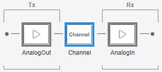
Channel Model Setup
Channel loss is set to
2dB (Note: this can vary given the specific UCIe Channel Reach of your system).Single-ended impedance is set to
50Ohms (Section 5.7.3)Target Frequency is set to the Nyquist frequency of
16GHz, which corresponds to 32GT/s with modulation set to NRZ.
Receiver Model Setup
The Rx AnalogIn block is configured as follows:
R (input resistance) is
50Ohms (Table 5-5).C (capacitance) is
0.125pF (Table 5-5).
The Rx CTLE block set up as follows:
4 configurations (0 to 3) and the associated GPZ Matrix is derived from the CTLE transfer equation provided (Section 5.4.3).
Note: A dedicated DFEClkFwd block that supports IBIS Clock Forwarding functionality will be added later after exporting to Simulink.
Determine CTLE GPZ Values
You can see from the loaded model that the Rx CTLE block contains multiple configurations to accommodate the dynamic range of this peaking filter. This is implemented using a gain-pole-zero matrix based on the transfer function provided by the UCIe specification (Section 5.4.3) as follows:
![]()
Where
wp2 = 2pi*DataRate,
wp1 = 2pi*DataRate/4,
and ADC is the DC Gain.
The following code block shows you one method to find a GPZ Matrix for the CTLE block using the transfer equation.
DCgain = 0:3;
ADC = 10.^(-DCgain/20);

datarate = 32e9; %Hz
p1 = datarate/4;
p2 = datarate;
wp1 = 2*pi*p1;
wp2 = 2*pi*p2;

f = linspace(0.1,20e9,1001);
w = 2*pi*f;
s = 1j*w;

H = zeros(length(ADC),length(f));

for ii = 1:length(ADC)
    H(ii,:) = wp2.*(s + ADC(ii)*wp1)./((s + wp1).*(s + wp2));
end

figure(1)
ax1(1) = subplot(211);
semilogx(f,db(H))
grid on
xlabel('Hz')
ylabel('dB')
title('Reference CTLE from UCIe 2.0, Section 5.4.3')
ax1(2) = subplot(212);
semilogx(f,unwrap(angle(H)))
grid on
xlabel('Hz')
ylabel('Radians')
linkaxes(ax1,'x')

%% Generate GPZ Matrix
% Define z1 for gpz matrix
z1 = ADC*p1;
% Define gpz matrix
gpz = zeros(length(ADC),4);
gpz(:,1) = -DCgain;
gpz(:,2) = -p1;
gpz(:,3) = -z1;
gpz(:,4) = -p2;
You can verify that the CTLE transfer function embedded in the system object matches the GPZ-matrix expression of that transfer function by using a visualization:
myctle = serdes.CTLE('Specification','GPZ Matrix','GPZ',gpz)
myctle =
  serdes.CTLE with properties:

   Main
             Mode: 2
    Specification: 'GPZ Matrix'
              GPZ: [4×4 double]
      SliceSelect: 0
     ConfigSelect: 0

  Show all properties
[~,H2]=response(myctle,f);
figure(2),clf,plot(f,db(H2),'r'),hold on,plot(f,db(H2),'b')

Note: You can also visualize the response by clicking the Add Plots and selecting CTLE Transfer Function from the drop-down menu.
You are now ready to export to Simulink for further customization, such as adding a dedicated DFEClkFwd block that supports IBIS Clock Forwarding and an entry for additional UCIe metrics such as Receiver Sensitivity.
Part 2: Export and Setup Single-Ended Data Models in Simulink
In SerDes Designer, click on the Export button to export the model ucie_txrx_data_se to Simulink to allow enhanced customization of each portion of the system.

Configure Data Transmitter Subsystem
The Tx subsystem contains an FFE block. You can configure the options available for controlling the FFE block by modifying its IBIS-AMI Parameter for presets in the IBIS-AMI Manager as follows.
Add New AMI Parameter
In the IBIS-AMI Manager, open the AMI - Tx tab. Then click on the FFE and add a new parameter named "ConfigSelect:"
In the edit dialog, enter the following:
Parameter name: ConfigSelect
Description: Tx FFE Tap Weights Configuration from UCIe Revision 2.0, Version 1.0
Usage: In
Type: Integer
Format: List
Default: 1
List values: [0 1 2]
List_Tip values: ["User Defined" "Setting 1" "Setting 2"]
Set the Current Value to Setting 1.
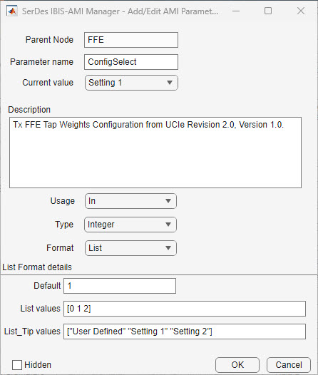
Click OK to save the new parameter. Note that a new Constant block named ConfigSelect was automatically added to the Tx FFE.
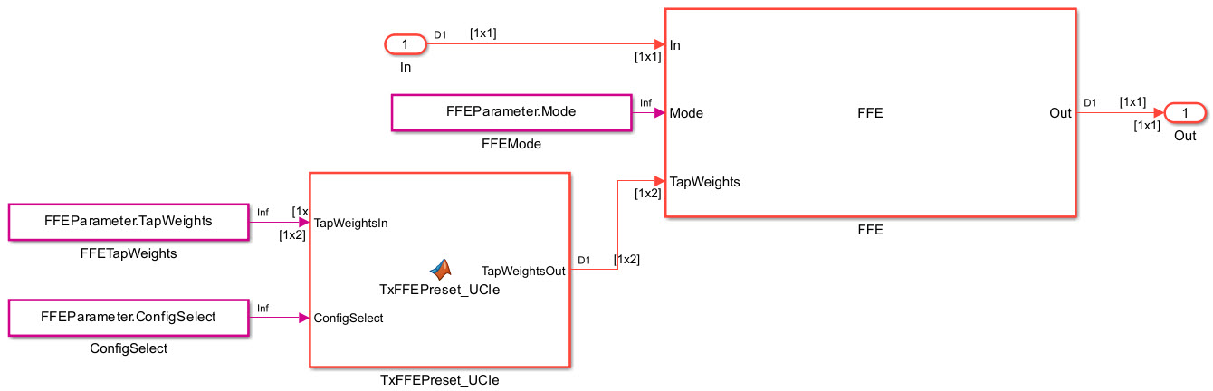
Update the Tx FFE Block
Next, look under the FFE block, and add a new MATLAB Function block named TxFFEPreset_UCIe. This block will be used to switch between the different Tx FFE presets based on the new IBIS_AMI parameter added above.
Copy/Paste the following code in the TxFFEPreset_UCIe MATLAB Function block, replacing the default contents:
function TapWeightsOut = TxFFEPreset_UCIe(TapWeightsIn, ConfigSelect)
% Derived from UCIe specification Revision 2.0, Version 1.0, Tx FFE. Table 5-4.
switch ConfigSelect
case 0 % User defined tap weights
TapWeightsOut = TapWeightsIn;
case 1 % Setting 1 (0.0dB de-emphasis)
TapWeightsOut = [1.0 0];
case 2 % Setting 2 (-2.2dB de-emphasis)
TapWeightsOut = [0.776 -0.224];
otherwise
TapWeightsOut = TapWeightsIn;
end
end
Delete the connection between the FFETapWeights block and the FFE.
Connect the FFETapWeights block to the
TapWeightsIninput to the function TxFFEPreset_UCIe.Connect the ConfigSelect block to the
ConfigSelectinput to the function TxFFEPreset_UCIe.Connect the output
TapWeightsOutof the TxFFEPreset_UCIe block to theTapWeightsinput of the FFE block.
You can see a diagram below of the completed subsystem:
Run Refresh Init on the Tx Init block to populate the new ConfigSelect AMI parameter:
Open the Tx block, then double-click on the Init block.
Click on Refresh Init.
Close the Init dialog.
Press Ctrl+D to compile the model and check for errors.
Configure the Data Receiver Subsystem
Next, you will need to add the capability of IBIS Clock Forwarding support in the receiver subsystem. This requires adding the IBIS AMI Reserved_Parameter "Rx_Use_Clock_Input" which is done automatically for you by the DFEClkFwd block. You can add this block with the following steps:
Double click on the Rx block
Click on the Library Browser
Navigate to the SerDes Toolbox section
And add an instance of the block DFEClkFwd
Then complete the path from WaveIn to CTLE block to DFEClkFwd block to WaveOut.

Next, set the DFE Mode to "Off" because we will not be using DFE feature of this block in this example (you will be using the IBIS-Clock-Forwarding feature provided by the DFEClkFwd block). Note: If you do wish to implement a 1-tap DFE per the UCI specification, you can set this up here.
You can ignore the various DFE tap settings, as these are defaults for the app and will not be used when set to "Off."

Then in the CDR tab, enter the following setting for receiver sensitivity:
Sensitivity (V) to
0.02(Table 5-5).Note: other CDR entries can be left to default settings.
Next, open the IBIS-AMI Manager and click on the AMI - Rx tab. A new Reserved_Parameter "Rx_Use_Clock_Input" has been added. You can set the drop-down for Current Value to "Wave."
Note: The DFE is set to off, so you can set the option Hidden to the following parameters to remove them from the AMI file.
DFEClkFwd.Mode
DFEClkFwd.ReferenceOffset
DFEClkFwd.PhaseOffset
DFEClkFwd.TapWeights

Close the IBIS-AMI Manger, then run Refresh Init on the Rx Init block to populate the new DFEClkFwd values.
Add Jitter for Single-Ended Data
Two jitter parameters are defined for the single-ended Tx data signals. No jitter parameters are defined for Rx data signals. From Table 5-3:
1-UI Total Jitter = 96mUI pk-pk
1-UI Deterministic Jitter (Dual Dirac) = 48mUI pk-pk
To add these jitter parameters to the Tx AMI model, open the IBIS-AMI Manager and click on the AMI - Tx tab. Click on the Reserved Parameters... button, check the boxes for Tx_Dj and Tx_Rj, and hit OK to add the jitter parameters to the list of Reserved_Parameters.
Tx_Dj
In IBIS-AMI Tx_Dj is defined as 1/2 the peak-to-peak value. Edit the Tx_Dj parameter and make the following changes:
Change the Format to Range.
Set the Typ and Min values to
0.Set the Max value to
0.024(half the pk-pk value)Set the Current value to
0.024
This setup will allow users to set any value for Tx_Dj from 0 to 0.024 UI.
Tx_Rj
We will model the remaining Jitter (Total Jitter - Deterministic Jitter) as Random Jitter. In IBIS-AMI Tx_Rj is defined as one standard deviation. Since Total Jitter is defined at a BER of 1e-15 (7.9 standard deviations), we need to divide the jitter value by 7.9 as well, making the full equation: (Total Jitter - Determinisitic Jitter) / 7.9 = (0.096 - 0.048) / 7.9 = 0.00608 UI.
Edit the Tx_Rj parameter and make the following changes:
Change the Format to Range.
Set the Typ and Min values to
0.Set the Max value to
0.00608Set the Current value to
0.00608
This setup will allow users to set any value for Tx_Rj from 0 to 0.00608 UI.
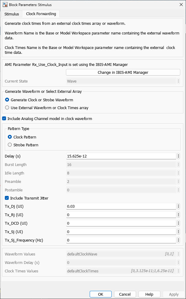
Configure the Data and Clock Forwarding Stimulus
Navigate to the Stimulus block and set the Waveform creation method to Serial PRBS, and set the PRBS order to 15.
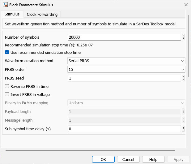
Note: if you click on the "Clock Forwarding" tab in the Stimulus dialog, you can see that the Current State is listed as "Wave" based on your selection above for Rx_Use_Clock Input in the IBIS-AMI Manager. You can also configure the following settings:
Generate Clock or Strobe Waveform: Enabled
Include Analog Channel model in clock waveform: Enabled
Pattern Type: Clock Pattern
Delay (s): 15.625e-12
Note: You can configure Delay value to optimize the location of the clock relative to the data. The setting of 15.625e-12 is exactly 1/2 UI.
To add clock jitter, click on Include Transmit Jitter and set the value for Tx_Dj to
0.03UI. (Table 5-3, 1/2 the mUI pk-pk value for "Tx Data/clock Differential Jtter).Note: Adding clock forwarding jitter only impacts the Simulink simulation. Jitter for the differential clock models will be added in Part 4.
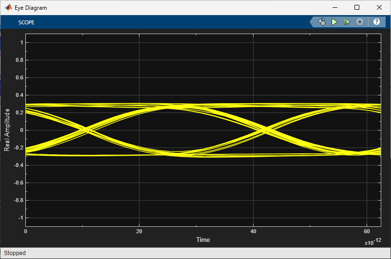
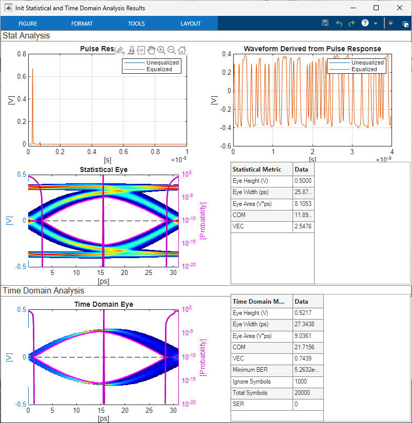
Run the system in Simulink. You should see results similar to the following:
Generate IBIS-AMI Models for Single-Ended Data
Next you will generate IBIS-AMI compliant model executables, IBIS and AMI files.
Open the dialog for the Configuration block and click on the SerDes IBIS-AMI Manager button. On the IBIS tab of the SerDes IBIS-AMI manager, the analog model values are converted to standard IBIS parameters that can be used by any IBIS-compliant simulator. On the AMI-Tx and AMI-Rx tabs, the reserved parameters are listed first followed by the model specific parameters, following the format of a typical AMI file.
Export IBIS-AMI Models
Select the Export tab in the SerDes IBIS-AMI manager dialog box.
Update the Tx model name to
ucie_data_cf_txUpdate the Rx model name to
ucie_data_cf_rxNote that the Tx and Rx corner percentage is set to
10%. This will scale the min/max analog model corner values by +/-10%.Verify that Dual model is selected for both the Tx and the Rx. This will create model executables that support both Statistical (Init) and Time Domain (GetWave) analysis.
Set the Tx model Bits to ignore value to
2since there are two taps in the Tx FFE.Set the Rx model Bits to ignore value to
1000as a reasonable value to enable Rx equalizer blocks to settle during time domain simulations.Verify that Both Tx and Rx are set to Export and that all files have been selected to be generated (IBIS file, AMI files, .dll files [Windows] and/or .so files [Unix/Linux]).
Set the IBIS file name to be
ucie_data_cf.ibsClick the Export button to generate models in the Target directory.
Part 3: Setup Tx and Rx Models for Differential Clock in SerDes Designer
Load the system model for clock by typing the following command in the MATLAB® command window to open the SerDes Designer model ucie_txrx_clk_ds.mat:
>> serdesDesigner('ucie_txrx_clk_ds')
Configuration Setup
Symbol Time is set to
31.25ps representing a data rate of 32 GT/s with NRZ modulation, which equates to a Nyquist frequency of 16GHz.Samples per Symbol is set to
16.Target BER is set to
1e-15(from Table 1-1 of the UCIe specification)Modulation is set to
NRZ.Signaling is set to
Differential(UCIe clock signals utilize differential signaling.
Transmitter Model Setup
The Tx AnalogOut block is configured as follows:
Voltage is
0.625V (Mid-point between Min value in Table 5-3 and Max recommended value from Section 1.5).Rise time is
12.5psR (output resistance) is
30Ohms (Table 5-3, Standard package).C (capacitance) is
0.125pF (Table 5-3).
Channel Model Setup
Channel loss is set to
2dB (Note: this can vary given the specific UCIe Channel Reach of your system).Differential impedance is set to
100Ohms.Target Frequency is set to the Nyquist frequency of
16GHz, which corresponds to 32GT/s with modulation set to NRZ.
Receiver Model Setup
The Rx AnalogIn block is configured as follows:
R (input resistance) is
50Ohms (Table 5-5).C (capacitance) is
0.125pF (Table 5-5).
You are now ready to export to Simulink for further customization.
Part 4: Export and Setup Differential Clock Models in Simulink
In SerDes Designer, click on the Export button to export the model ucie_txrx_clk_ds to Simulink to allow customization of each portion of the system.

Configure the Clock Transmitter Subsystem
Unlike the data transmitter, in UCIe the differential clock transmitter does not have any equalization, so an algorithmic (AMI) model is not required. However, it is highly recommended that a "pass through" transmitter model be generated anyway so that the Tx AMI file can supply any jitter or modulation information that may be required for simulations to run properly. In this instance, the transmitter AMI model will not modify the signal in any way.
Configure the Clock Receiver Subsystem
Next you will set up the clock receiver subsystem to add a zero-crossing detector to output clock times for IBIS Clock Forwarding support. Instead of using a CDR, which generates clock times based on the incoming data signal, for clock forwarding we want to use the exact time that the differential clock signal crosses zero volts. When Rx_Use_Clock_input is set to Times, these zero-crossing times will be used directly by the data receiver model.
Open the Rx subsystem. Put down a pass-thru block and rename the pass-thru block to ClockDetect.

Add New AMI Parameters
Open the IBIS-AMI Manager. On the AMI - Rx tab, you will see that ClockDetect is now listed under the Model_Specific section.
The ClockDetect pass-through block requires two new IBIS Parameters. On the AMI - Rx tab in the IBIS-AMI Manager, add new parameters under the Model_Specific entry for ClockDetect as follows:
Add new parameter DQS_Preamble:
Parameter name: DQS_Preamble
Description: Number of DQS transitions to skip before outputting clock times during a DQS burst. Currently requires at least 4 DQS UI between bursts. 1tCK = 2 DQS UI.
Usage: In
Type: Integer
Format: List
Default: 0
List values: [0 1 2 3 4]
List_Tip values: ["0tCK" "1tCK" "2tCK" "3tCK" "4tCK"]
Current value: 0tCK
Hidden: Check Enabled
Note: The Hidden option is being selected to hard-code 0 (0tCK) as the default for this model. This function is capable of accommodating DDR5 and other DDR standards, but for UCIe this is a clock signal and no preamble is used.

Add new parameter Strobe_or_Clock:
Parameter name: Strobe_or_Clock
Description: Strobe or Clock signal. A Strobe signal returns clock times every edge (DDR) while a Clock signal only returns clock times on rising edges (SDR).
Usage: In
Type: Integer
Format: List
Default: 0
List values: [0 1]
List_Tip values: ["Strobe" "Clock"]
Current value: Strobe
Hidden: Check Enabled
Note: The Hidden option is being selected to hard-code 0 (Strobe) as the default for this model. This function is capable of accommodating both DDR and SDR standards, but for UCIe this clock signal always output clock_times on both rising and falling edges (DDR).

Although the above parameters are never used by Init, it is good practice to always run Refresh Init when new AMI parameters are added to the model. Close the IBIS-AMI Manger, then run Refresh Init on the Rx Init block to populate the new parameters.
Update the ClockDetect Pass-Through Block
To create the zero-crossing detector to support IBIS Clock Forwarding functionality, you will use the function DQSClock.m attached to this example.
Note: A detailed discussion of this function is beyond scope of this example, but a link to the source example Design IBIS-AMI Models to Support Clock Forwarding is provided below.
Look under the ClockDetect Pass-through block where you should see the two new AMI parameters that were just created.
Add a MATLAB Function block called DQSClock. Also add an IBIS-AMI clock_times block from the Library Browser for SerDes Toolbox. The DQSClock MATLAB function block will contain the MATLAB code for the zero-crossing detector, while the IBIS-AMI clock_times block will be used to output the resulting clock times to AMI_Parameters_Out per the IBIS-AMI spec.
Open the DQSClock MATLAB function block and completely replace the contents with the contents of DQSClock.m attached to this example. The values for two of the inputs to this function, SymbolTime and SampleInterval, are inherited from the Model Workspace and therefore do not need to show up as nodes on the MATLAB Function block. To remove these nodes from the MATLAB Function block:
Save the model.
In the MATLAB function signature highlight the parameter SymbolTime.
Right-click the parameter and select
Data Scope for "SymbolTime"from the right-click menu.Change the Data Scope from
InputtoParameter.Repeat this process for SampleInterval.
You should now see that these two input parameters have been removed from the function block on the Simulink canvas.
Now, you can connect the subsystem components as follows:
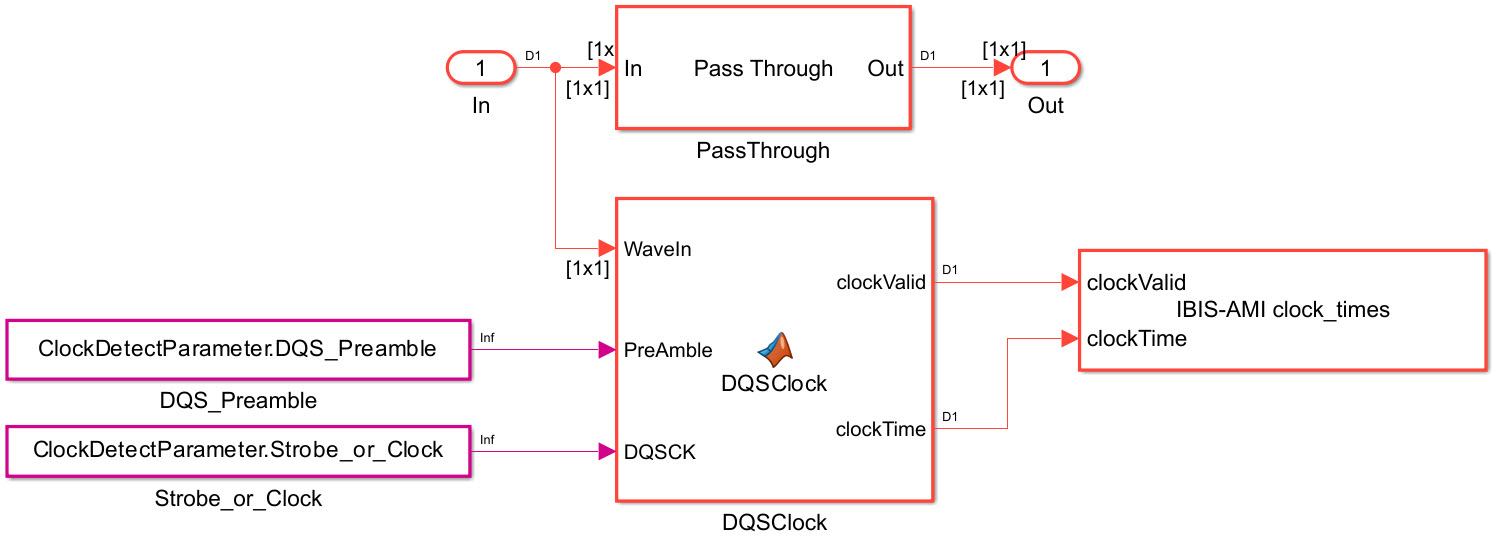
Connect In to the WaveIn input to the DQSClock block.
Connect DQS_Preamble to the PreAmble input of the DQSClock block.
Connect Strobe_or_Clock to the DQSCK input of the DQSClock block.
Connect the clockValid output to the clockValid input of the IBIS-AMI clock_times block.
Connect the clockTime output to the clockTime input of the IBIS-AMI clock_times block.
Below is an example of how the subsystem should appear:
Set Clock Offset
Per the IBIS Specification, clock times output from an Rx AMI model must be exactly symbol_time/2 before the input data signal is sampled. However, for clock forwarding, the actual clock_times are output from the clock Rx AMI model so that the data Rx AMI can use them directly. Note: If this clock model is used in isolation, the output clock_times passed to the EDA tool will not have the required symbol_time/2 offset.
To bypass this offset, double-click on the IBIS-AMI clock_times block and uncheck the box for the parameter Enable IBIS-AMI Offset.

Press Ctrl+D to compile the model and check for errors.
Add Jitter for Differential Clock
One jitter parameter is defined for the differential clock Tx clock signal and one for the Rx clock signal. We will model both of these parameters with Deterministic Jitter.
Tx Data/clock Differential Jitter = 60mUI pk-pk (Table 5-3)
Rx Data/clock Total Differential Jitter = 60mUI pk-pk (Table 5-5)
To add these jitter parameters to the Tx AMI model, open the IBIS-AMI Manager and click on the AMI - Tx tab. Click on the Reserved Parameters... button, check the box for Tx_Dj, and hit OK to add the jitter parameter to the list of Reserved_Parameters.
Tx_Dj
In IBIS-AMI Tx_Dj is defined as 1/2 the peak-to-peak value. Edit the Tx_Dj parameter and make the following changes:
Change the Format to Range.
Set the Typ and Min values to
0.Set the Max value to
0.030(half the pk-pk value)Set the Current value to
0.030
This setup will allow users to set any value for Tx_Dj from 0 to 0.030 UI.
Rx_Dj
In the IBIS-AMI Manager and click on the AMI - Rx tab. Click on the Reserved Parameters... button, check the box for Rx_Dj, and hit OK.
In IBIS-AMI Rx_Dj is defined as 1/2 the peak-to-peak value. Edit the Rx_Dj parameter and make the following changes:
Change the Format to Range.
Set the Typ and Min values to
0.Set the Max value to
0.030(half the pk-pk value)Set the Current value to
0.030
This setup will allow users to set any value for Rx_Dj from 0 to 0.030 UI.
Configure Clock Stimulus
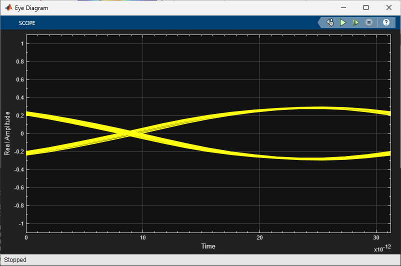
You can configure the Stimulus block such that it is representative of a clock signal as follows:
Waveform Creation method: Binary Pattern
Binary pattern: [0 1 0 1 0 1 0 1]

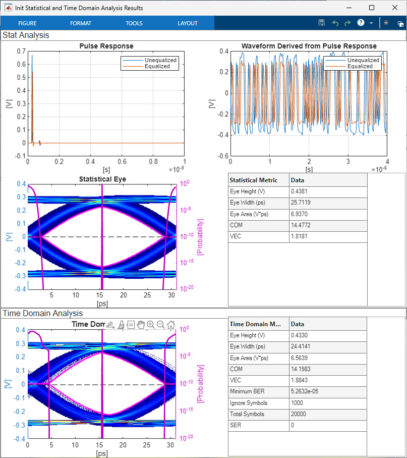
Run the system in Simulink. You should see results similar to the following:
Note: Given that a binary pattern is being implemented, it is recommened to set the option in the Eye Diagram plot for "Symbols per trace" to 1 In Scope Settings to optimize the visualization.
Generate IBIS-AMI Models for Differential Clock
Next you will generate IBIS-AMI compliant model executables, IBIS and AMI files.
Open the dialog for the Configuration block and click on the SerDes IBIS-AMI Manager button. On the IBIS tab of the SerDes IBIS-AMI manager, the analog model values are converted to standard IBIS parameters that can be used by any IBIS-compliant simulator. On the AMI-Tx and AMI-Rx tabs, the reserved parameters are listed first followed by the model specific parameters, following the format of a typical AMI file.
Export IBIS-AMI Models
Select the Export tab in the SerDes IBIS-AMI manager dialog box.
Update the Tx model name to
ucie_clk_cf_txUpdate the Rx model name to
ucie_clk_cf_rxNote that the Tx and Rx corner percentage is set to
10%. This will scale the min/max analog model corner values by +/-10%.Verify that Dual model is selected for both the Tx and the Rx. This will create model executables that support both statistical (Init) and time domain (GetWave) analysis.
Set the Rx model Bits to ignore value to
1000as a reasonable value to enable Rx blocks to settle during time domain simulations.Verify that Both Tx and Rx are set to Export and that all files have been selected to be generated (IBIS file, AMI files, .dll files [Windows] and/or .so files [Unix/Linux]).
Set the IBIS file name to
ucie_clk_cf.ibsClick the Export button to generate models in the Target directory.
Test Generated IBIS-AMI Models
The UCIe 2.0 transmitter and receiver IBIS-AMI models are now complete and ready to be utilized within Parallel Link Designer from Signal Integrity Toolbox, or any industry standard EDA tool capable of IBIS-AMI simulation with support for IBIS Clock Forwarding.
Limitations
Package Models: No package models have been included here. Package models for your specific implementation should be added following the IBIS conventions.
Analog Models: Per the UCIe specification, the Tx signal swing can vary from 0.4V (Table 5-3) to 0.85V (Section 1.5). These are not typ/min/max values that vary with Process, Voltage and Temperature (PVT), but rather absolute min/max values. The analog models generated in this example use a nominal voltage swing of 0.625 V (mid-point between the minimum and maximum recommended values), with a +/-10% varation for PVT. If your Tx model uses a different nominal voltage, the Tx analog Vswing parameter should be adjusted accordingly.
References
[1] UCIe Revision 2.0 Specification, Version 1.0: https://www.uciexpress.org/
[2] IBIS 7.2 Specification, including definition of Clock Forwarding implementation in IBIS-AMI models: https://ibis.org/ver7.2/ver7_2.pdf
See Also
SerDes Designer | FFE | CTLE | CDR
Related Topics
References
[1] UCIe Version 1.0 Specification, Revision 1.1: https://www.uciexpress.org/
[2] IBIS 7.2 Specification, including definition of Clock Forwarding implementation in IBIS-AMI models: https://ibis.org/ver7.2/ver7_2.pdf
See Also
SerDes Designer | FFE | CTLE | CDR