LPDDR5X IBIS-AMI Models with Clock Forwarding
This example shows how to create IBIS-AMI models for Low Power Double Data Rate 5X (LPDDR 5X) transmitter and receiver for signals including Write-Clock (WCK) and Data (DQ) using the library blocks in SerDes Toolbox™. The IBIS-AMI models generated by this example utilize IBIS Clock Forwarding functionality which can be imported and simulated in Parallel Link Designer from Signal Integrity Toolbox™. Additional signals are outlined at the end of this example.
Create Tx and Rx Models for Single-Ended Data and Differential Clock Signals for Double Data Rate Write
This example shows how to create transmitter and receiver for Write-Clock (WCK) and Data (DQ) for a LPDDR5X system Write Transaction, using the SerDes Designer app to later create IBIS-AMI models. You will see how the system can then be exported to Simulink® for further customization. You can later build other signal models by configuring various settings using values from the LPDDR5X specification (see reference section below) in both the SerDes Designer app and in Simulink.
Part 1: Setup Tx and Rx Models for Single-Ended Data in SerDes Designer
You can load the system model for the LPDDR5X data signal by typing the following command in the MATLAB® command window to open the SerDes Designer model lpddr5x_data.mat:
>> serdesDesigner('lpddr5x_data');

Configuration Setup
Symbol Time is set to 117.2 ps representing a WCK = 4CK-driven DQ double data rate of LPDDR5X-8533, which equates to a Nyquist frequency of 4.266GHz.
Target BER is set to
100e-18.Samples per Symbol is set to 16 (default).
Modulation is set to NRZ.
Signaling is set to Single-ended.
Transmitter Model Setup
Tx FFE is defined as having 2 cursors: one main tap and one post-tap. The initial setting is as follows:
Tap Weights is
[1 0](See JESD 209-5C, section 7.7.11 - Pre-Emphasis for DQ Output).Set Mode to off.
Note: Specific tap presets will be configured to be selectable options later in this example after the system is exported to Simulink.
The Tx AnalogOut block is configured as follows:
Voltage is 0.5 V.
Rise time is 40 ps.
R (output resistance) is 40 Ohms (to represent a transmitter with 40-Ohm drive strength)
C (capacitance) is 0.7 pF (See range of values, JESD 209-5C, Table 436).
Channel Model Setup
Channel loss is set to 3 dB (Note: this can vary given the specific design of your system).
Single-ended impedance is set to 40 Ohms.
Target Frequency is set to the Nyquist frequency of 4.266 GHz, which corresponds to LPDDR5X-8533 with modulation set to NRZ.
Receiver Model Setup
The Rx AnalogIn block is configured as follows:
R (input resistance) is 100e6 Ohms (to represent high-impedance receiver, with on-die termination (ODT) set to none/disabled).
C (capacitance) is 0.7 pF (See range of values, JESD 209-5C, Table 436).
The Rx DFECDR block set up as follows:
1-Tap DFE with negative-feedback only; note that DFE is an optional feature (See JESD 209-5C, section 7.7.7).
Set Initial tap weights (V) to 0.
Set Minimum tap value (V) to -0.100.
Set Maximum tap value (V) to 0.
Set Mode to off.
Note: The DFECDR offers an option for "2X Taps." Check this option to have pulse response values match convention used by JEDEC. Clear this option to use pulse response values directly from the plot.
Note: This block will be replaced by the DFEClkFwd block to support IBIS Clock Forwarding functionality after exporting to Simulink.
You are now ready to export to Simulink for further customization, including support for IBIS Clock Forwarding.
Part 2: Export Single-Ended Data Models to Simulink
In SerDes Designer, click on Export in the toolstrip to export the model lpddr5x_data to Simulink.
Configure Data Transmitter Subsystem
The Tx subsystem contains a an FFE block and which can be customized in the SerDes IBIS-AMI Manager as follows to add the capability to select FFE presets. We will defined 2 presets and also give the ability to enter a User Defined value, so that these are selectable options in an IBIS Simulation tool to help the user configure the model:
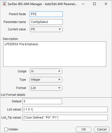
In the IBIS-AMI Manager, open the AMI - Tx tab. Then click on the FFE and create a new parameter "ConfigSelect:"
In the edit dialog box, enter the following:
Parameter name: ConfigSelect
Description: Tx FFE Tap Weights Configuration
Usage: In
Type: Integer
Format: List
Default: 0
List values: [-1 0 1]
List_Tip values: ["User Defined" "P0" "P1"]
Then set the Current Value to P0.
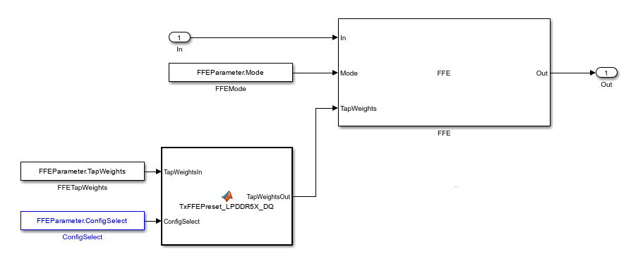
Next, you will see a new FFE block has been created and you can create a new MATLAB function that can switch based on the new IBIS-AMI parameter as follows:
Click on the canvas and create a MATLAB function named TxFFEPreset_LPDDR5X_DQ.
The following code block shows an option for how to provide a selector within the IBIS-AMI model:
Note: The value for P0 is the default. The value given for P1 is an example, which may vary depending on your specific SDRAM device. The value from User Defined allows any custom value to be used when using the IBIS-AMI model. Additional presets can be added as needed.
Note: Presets should be normalized to 1.0.
function TapWeightsOut = TxFFEPreset_LPDDR5X_DQ(TapWeightsIn, ConfigSelect)
switch ConfigSelect
case -1 % User defined tap weights
TapWeightsOut = TapWeightsIn;
case 0 % Preset Configuration: P0
TapWeightsOut = [1.0 0.0];
case 1 % Preset Configuration: P1
TapWeightsOut = [0.9 -0.1];
otherwise
TapWeightsOut = TapWeightsIn;
end
end
Connect the FFEParameter.TapWeights constant block to the TapWeightsIn input to the function TxFFEPreset_LPDDR5X_DQ.
Connect the FFEParameter.ConfigSelect constant block to the ConfigSelect input to the function TxFFEPreset_LPDDR5X_DQ.
Connect the output TapWeightsOut of the TxFFEPreset_LPDDR5X_DQ block to the TapWeights input of the FFE block.
You can see a diagram below of the completed subsystem:
Note: You will need to repeat the above process for the Tx Init as well.
Configure Analog Channel
Next, you can open the Analog Channel block to confirm the settings exported from SerDes Designer during the previous section:
Channel Model: Loss Model
Target Frequency: 4.266e9 Hz
Loss (dB): 3
Impedance (Ohms): 40
Tx R (Ohms): 40
Tx C (F): 700e-15
Rx R(Ohms): 100e6
Rx C(F): 700e-15
Rise Time (s): 40e-12
Voltage (V): 0.5
Configure Data Receiver Subsystem for IBIS Clock Forwarding
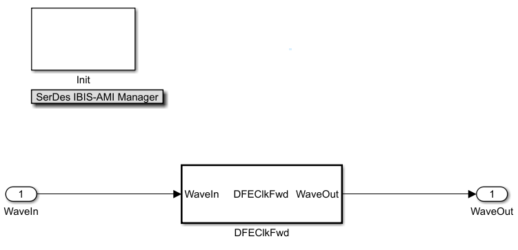
Next, you will need to add the capability of IBIS Clock Forwarding support in the receiver subsystem. Part of this involves adding the IBIS AMI Reserved_Parameter "Rx_Use_Clock_Input." This is enabled automatically by a DFEClkFwd block: you can change the DFECDR block to a DFEClkFwd block with the following steps:
Double click on the Rx block
Click on the Library Browser
Navigate to the SerDes Toolbox section
And add an instance of the block DFEClkFwd
Then delete the original DFECDR block so that the DFEClkFwd block connects WaveIn to WaveOut.
After replacing the DFECDR block with the DFEClkFwd block, you must click on Refresh Init to update the Rx Initialize function with the new block.
Note: You can set the DFE tap settings for use as an optional feature as was done previously in the DFECDR:
Set Mode to Off.
Set Initial tap weights (V) to 0.
Leave Adaptive gain set to default of 3.0e-6.
Leave Adaptive step size (V) set to default of 1.0e-6.
Set Minimum tap value (V) to -0.100.
Set Maximum tap value (V) to 0.
Set Mode to "Off" to allow the user to enable later during simulation.
Note: the DFECDR offers an option for "2X Taps." Check this option to have pulse response values match convention used by JEDEC DDRx specifications. Clear this option to use pulse response values directly from the plot.

Note: in the CDR tab, the entries can be left to default settings. The CDR will only be used when IBIS Clock Forwarding is not used by the Rx model.
Next, open the IBIS-AMI Manager, and click on the AMI - Rx tab. A new Reserved_Parameter "Rx_Use_Clock_Input" has been added. You can set the drop-down for Current Value to "Wave" to use a waveform input to clock the Rx. For more information on this AMI parameter see the IBIS specification.

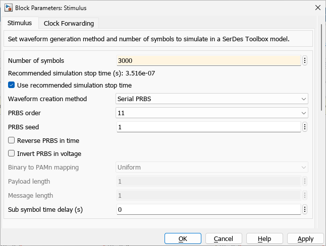
Configure Data Stimulus
You can navigate to the Stimulus block and set the Waveform creation method to Serial PRBS (Note: PRBS is not required- in fact, in real LPDDR5X systems, some symbol-ordering are prohibited so this would represent a pessimistic simulation- what is required is to utilize a data-like symbol stream of 11101001... the goal is to avoid a clock-like symbol stream of 101010... in order to more closely represent Inter-Symbol Interference or ISI).
Note: the default for Number of symbols is 20000, but you can utilize a smaller value by approximately a factor-of-ten to speed-up simulation run times while still retaining sufficient symbols, such as 3000.
Note: if you click on the "Clock Forwarding" tab in the Stimulus window, you can see that the Current State is listed as "Wave" based on your selection above for Rx_Use_Clock Input in the IBIS-AMI Manager. You can also configure the following settings:
Generate Clock or Strobe Waveform: Enabled
Include Analog Channel model in clock waveform: Enabled
Pattern Type: Clock Pattern
Delay (s): 58.6e-12
Note: You can configure Delay value to optimize the location of the clock PDF in the plot. You should observe that a value of 58.6 ps centers the location of the clock PDF for this setup because the Symbol Time of 117.2 ps is dominant (58.6 ps is half of this value), whereas this value may need to be optimized or altered depending on actual channel length when IBIS-AMI models with Clock Forwarding are utilized in an IBIS simulator.

Run the system in Simulink.
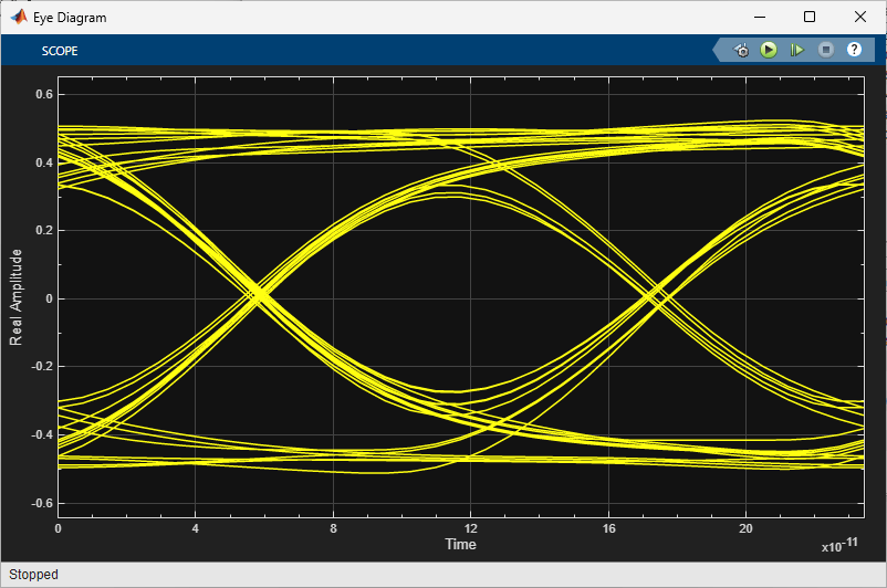
Note: Above figure shows Time-Domain waveform during and after simulation completion.
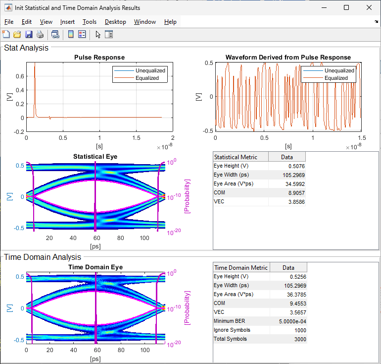
Note: Above figure shows a 3000-symbol simulation result set.
Generate and Export IBIS-AMI Models for Single-Ended Data
The next part of this example takes the customized Simulink model and generates IBIS-AMI compliant model executables, IBIS and AMI files.
Open the SerDes IBIS-AMI Manager. In the IBIS tab inside the SerDes IBIS-AMI manager dialog box, the analog model values are converted to standard IBIS parameters that can be used by any industry standard simulator. In the AMI-Tx and AMI-Rx tabs in the SerDes IBIS-AMI manager dialog box, the reserved parameters are listed first followed by the model specific parameters following the format of a typical AMI file.Export IBIS-AMI Models
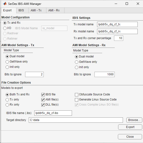
Select the Export tab in the SerDes IBIS-AMI manager dialog box.
Update the Tx model name to lpddr5x_dq_cf_tx
Update the Rx model name to lpddr5x_dq_cf_rx
Note that the Tx and Rx corner percentage is set to 10%. This will scale the min/max analog model corner values by +/-10%.
Verify that Dual model is selected for both the Tx and the Rx. This will create model executables that support both statistical (Init) and time domain (GetWave) analysis.
Set the Tx model Bits to ignore value to 2 since there is 1 main tap and 1 post tap in the Tx FFE.
Set the Rx model Bits to ignore value to 1000 as a reasonable value to enable Rx equalizer blocks to settle during time domain simulations.
Verify that Both Tx and Rx are set to Export and that all files have been selected to be generated (IBIS file, AMI files, .dll files [Windows] and/or .so files [Unix/Linux]).
Set the IBIS file name to be lpddr5x_dq_cf.ibs
You can now observe the IBIS-AMI manager looks as follows, where your system is ready to export IBIS-AMI models.
Once verified, you can click the Export button to generate models in the Target directory.
Part 3: Setup Tx and Rx Models for Differential Write-Clock in SerDes Designer
You can load the SerDes Designer model for clock by typing the following command in the MATLAB command window to open the model lpddr5x_wck.mat:
You will observe that WCK is a differential signal and does not include equalization, this is because equalization is only specified for Data-class signals for LPDDR5X (See JESD 209-5C specification).
>> serdesDesigner('lpddr5x_wck');

Configuration Setup
Symbol Time is set to 117.2 ps representing a WCK = 4CK double data rate of LPDDR5X-8533, which equates to a Nyquist frequency of 4.266GHz.
Target BER is set to
1e-16.Samples per Symbol is set to 16 (default).
Modulation is set to NRZ.
Signaling is set to Differential.
Transmitter Model Setup
The Tx AnalogOut block is configured as follows:
Voltage is 0.5V.
Rise time is 40 ps.
R (output resistance) is 40 Ohms (to represent a transmitter with 40-Ohm drive strength).
C (capacitance) is 0.7 pF (See JESD 209-5C, Table 436).
Channel Model Setup
Channel loss is set to 3 dB (Note: this can vary given the specific design of your system).
Differential impedance is set to 80 Ohms.
Target Frequency is set to the Nyquist frequency of 4.266 GHz, which corresponds to LPDDR5X-8533 with modulation set to NRZ.
Receiver Model Setup
The Rx AnalogIn block is configured as follows:
R (input resistance) is 100e6 Ohms (to represent a high-impedance receiver with ODT off or disabled).
C (capacitance) is 0.7 pF (See JESD 209-5C, Table 436).
Part 4: Exporting Differential Write-Clock Models to Simulink
Setup Differential Write-Clock Model
In this section, you will continue this workflow by exporting the differential write-clock (WCK) model to Simulink. In EDA tools for IBIS-AMI simulation, the clock and data are expected to be implemented as a pair to support IBIS Clock Forwarding simulation.
Click on Export in the toolstrip to launch Simulink with the differential clock system model lpddr5x_wck.

Configure Transmitter Subsystem for Write-Clock
You can look at the components of the Tx subsystem by double-clicking on the Tx block, and you can see the system has no equalization components. This is because equalization is only specified for Data-class signals for LPDDR5X (See JESD 209-5C specification).

Configure Receiver Subsystem for Write-Clock
Next you will setup the clock receiver subsystem to add a zero-crossing detector to output clock times for IBIS Clock Forwarding support. Double-click on the Rx block to open the Rx subsystem. Put down a pass-thru block. Rename the pass-thru block ClockDetect.
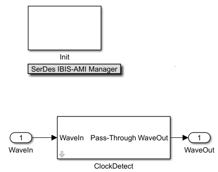
Go into the IBIS-AMI Manager. On the AMI-Rx tab, you can see that ClockDetect is now listed under the Model_Specific section. To support IBIS Clock Forwarding functionality, you will use a reference function DQSClock.m attached to this example. The function DQSClock.m utilizes specific IBIS Parameters. Note: A detailed discussion of this function is beyond scope of this example, but a reference for the source example Design IBIS-AMI Models to Support Clock Forwarding is provided below.
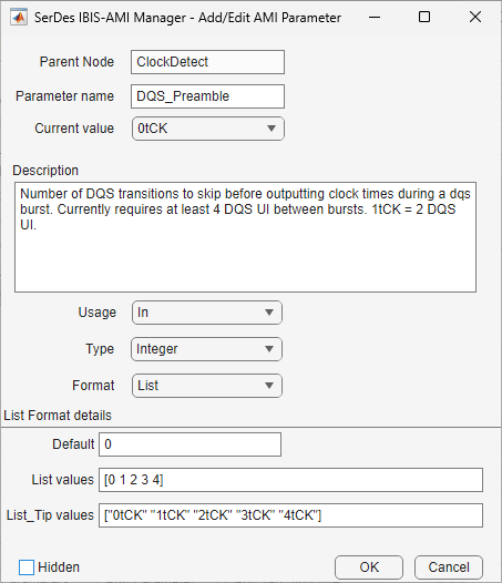
Navigate to the AMI - Rx tab in the IBIS-AMI Manager, and create new Parameters for the following under the Model_Specific entry for ClockDetect that was created above.
DQS_Preamble
Strobe_or_Clock
For the Parameter DQS_Preamble, create the following values:
Parent Node: ClockDetect
Parameter name: DQS_Preamble
Description: Number of DQS transitions to skip before outputting clock times during a dqs burst. Currently requires at least 4 DQS UI between bursts. 1tCK = 2 DQS UI.
Usage: In
Type: Integer
Format: List
Default: 0
List values: [0 1 2 3 4]
List_Tip values: ["0tCK" "1tCK" "2tCK" "3tCK" "4tCK"]
Current value: 0tCK
Hidden: Disabled
Note: this Parameter is capable of accommodating DDR5 and other DDR or SDR standards that may utilize IBIS Clock Forwarding.
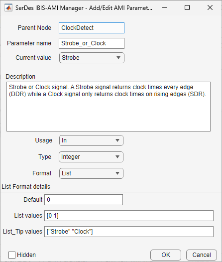
For the Parameter Strobe_or_Clock, create the following values:
Parent Node: ClockDetect
Parameter name: Strobe_or_Clock
Description: Strobe or Clock signal. A Strobe signal returns clock times every edge (DDR) while a Clock signal only returns clock times on rising edges (SDR).
Usage: In
Type: Integer
Format: List
Default: 0
List values: [0 1]
List_Tip values: ["Strobe" "Clock"]
Current value: Strobe
Hidden: Disabled
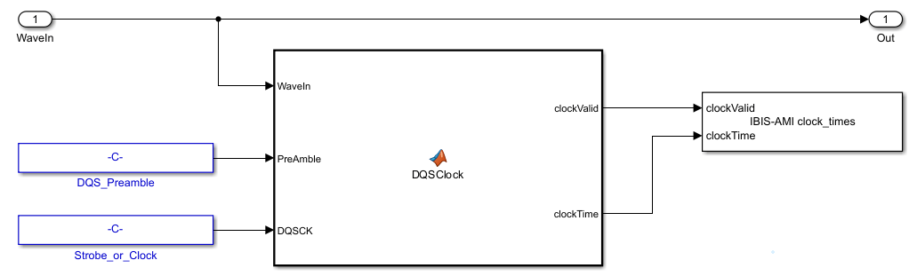
Now that you have created these Parameters, look under the Pass-through block and follow these steps to setup IBIS Clock Forwarding support. This will involved utilization of a code block contained in the attached file DQSClock.m.
Add a MATLAB Function block to call
DQSClock.m. Note: Alternatively, you can copy/paste the contents of this file into the code editor to define this function block.Make sure that the Data Scope for SampleInterval and SymbolTime is set to "Parameter" by right-clicking on each in the function header. Note: You may need to save the Simulink model before setting the Data Scope.
Place an IBIS-AMI clock_times block from the Library Browser for SerDes Toolbox.
Delete the PassThrough System object™.
Now you can connect the subsystem components as follows:
Connect WaveIn to Out
Connect WaveIn also to WaveIn input to the DQSClock block.
Connect DQS_Preamble to the PreAmble input of the DQSClock block.
Connect Strobe_or_Clock to the DQSCK input of the DQSClock block.
Connect clockValid output to the clockValid input of the IBIS-AMI clock_times block.
Connect clockTime output to the clockTime input of the IBIS-AMI clock_times block.
Below is an example of how the subsystem should appear:
Next, set the following Block Parameters for IBIS-AMI clock_times block:
Enable IBIS-AMI Offset: Disabled

Note: In order to properly output the clock crossing times to support Clock Forwarding, you must clear Enable IBIS-AMI Offset. Further explanation is provided in the example Design IBIS-AMI Models to Support Clock Forwarding in the reference section below.
Note: In the receiver subsystem, click on Refresh Init to update the Rx Initialize function with the new blocks and their settings.
Configuration Block Settings for Clock Subsystem
You can confirm the Configuration block settings are as follows:
Symbol time (s): 117.2e-12
Samples per symbol: 16
Target BER: 1e-16
Modulation: NRZ
Signaling: Differential
Eye Diagram Clock: Clocked

Configure Clock Stimulus
You can configure the Stimulus block such that it is representative of a clock signal as follows:
Number of symbols: 3000 (Note: the default is 20000, but a value of 3000 allows for quicker simulation times)
Waveform Creation method: Binary Pattern
Binary pattern: [0 1 0 1 0 1 0 1]
Leave Sub symbol time delay (s) to default value of 0

You can now run the system in Simulink.
Note: Given that a binary pattern is being used for stimulus, it is recommended in the Time Domain plot settings menu, to set the option "Symbols per trace" to 1 to optimize visualization.

Note: Above figure shows Time-Domain waveform with "Symbols per trace" set to 2.

Note: Above figure shows Time-Domain waveform with "Symbols per trace" set to 1.
Generate and Export IBIS-AMI Models for Differential Write-Clock
The next part of this example takes the customized Simulink model and generates IBIS-AMI compliant model executables, IBIS and AMI files.
Open the Block Parameter dialog box for the Configuration block and click on the SerDes IBIS-AMI Manager button. In the IBIS tab inside the SerDes IBIS-AMI manager dialog box, the analog model values are converted to standard IBIS parameters that can be used by any industry standard simulator. In the AMI-Tx and AMI-Rx tabs in the SerDes IBIS-AMI manager dialog box, the reserved parameters are listed first followed by the model specific parameters following the format of a typical AMI file.
Export IBIS-AMI Models
Select the Export tab in the SerDes IBIS-AMI manager dialog box.
Update the Tx model name to lpddr5x_wck_cf_tx
Update the Rx model name to lpddr5x_wck_cf_rx
Note that the Tx and Rx corner percentage is set to 10%. This will scale the min/max analog model corner values by +/-10%.
Verify that Dual model is selected for both the Tx and the Rx. This will create model executables that support both statistical (Init) and time domain (GetWave) analysis.
Set the Tx model Bits to ignore value to 0 since there is no equalization in the WCK transmitter.
Set the Rx model Bits to ignore value to 1000 as a reasonable value to enable Rx blocks to settle during time domain simulations.
Verify that Both Tx and Rx are set to Export and that all files have been selected to be generated (IBIS file, AMI files, .dll files [Windows] and/or .so files [Unix/Linux]).
Set the IBIS file name to be lpddr5x_wck_cf.ibs
You can now observe the IBIS-AMI manager looks as follows, where your system is ready to export IBIS-AMI models.
Click the Export button to generate models in the Target directory.

Building Signal Models for CK, CA, and RDQS
It is beyond scope of this example to illustrate each specific signal for an LPDDR5X interface. To support Write transactions, you have seen how to build DQ which includes Tx and Rx equalization, and how to build WCK differential models. The remainder of the signal types may be considered as an exercise for you to conduct. For example, to support Read transactions, you would create a differential RDQS as outlined below. The following signals are mapped out by the LPDDR5X specification as follows:
DQ: Single-ended Data for Write and Read Transactions as defined in above sections.
WCK_t, WCK_c: Differential DDR Clock for DQ-bus Write Transactions as defined in above sections. Includes Tx FFE and Rx DFE as optional features.
RDQS_t,RDQS_c: Differential Strobe for DQ-bus Read Transactions: Same impedance and capacitance as WCK, also includes Tx FFE and Rx DFE as optional features. For example, this could be generated by following the steps for DQ above, except selecting "Differential" signaling instead of "Single-Ended." In silicon devices, this is generated from WCK by the SDRAM.
CK_t,CK_c: Differential Clock for Address/Control Write Transactions: Same impedance and capacitance as WCK, but operates at 1/4 rate (Table 436). No equalization specified.
CA: Single-ended Address/Control for Write Transactions: Same impedance and capacitance as DQ, but operates at 1/4 rate (Table 436). No equalization specified.
CS: Chip Select signal (Section 15.5). No equalization specified.
Modify IBIS File to Add Model Selector and Add ODT to IBIS Input Models
To add ODT to IBIS Input Models, is beyond scope for this example, but the following steps outline how you can implement the IBIS Keywords for [Rgnd], [Rpower], [Rac], and [Cac] within the [Model] section of the IBIS file:
You can create a
[Model Selector]in your IBIS file that allows selection between multiple [Model] sections within an IBIS file.Then duplicate the [Model] for your Input buffer for each value of ODT.
And add different values for ODT to each: disabled or by adding various values for [Rac] and [Cac].
Reference: IBIS 7.2 specification (or newer) for example, under Keywords: [Rgnd], [Rpower], [Rac], [Cac] (also reference Figure 14 of the IBIS 7.2 Specification).
Example: The following shows an IBIS 7.2 implementation of "ODT set to 40-ohms pull-down" Rtt value per JESD209-5C for a
[Model] DQ_ODT40contained in an IBIS file:
[Model] DQ_ODT40
Model_type Input
[Rgnd] 40
Note: IBIS Keywords suchs [Rgnd], [Rac], [Cac], etc. act as supporting SPICE models for features such as ODT using in this model deck, and require support for IBIS 7.2 or newer within an IBIS simulation EDA tool.
Test Generated IBIS-AMI Models
The LPDDR5X transmitter and receiver IBIS-AMI models for single-ended data (DQ) and differential write-clock (WCK) for Write Transactions are now complete and ready to be utilized within Parallel Link Designer from Signal Integrity Toolbox, or any industry EDA tool capable of IBIS-AMI simulation with support for IBIS Clock Forwarding.
References
[1] JEDEC Standard, Low Power Double Data Rate (LPDDR) 5/5X, JESD209-5C: https://www.jedec.org/
[2] IBIS 7.2 Specification, including definition of Clock Forwarding implementation in IBIS-AMI models: https://ibis.org/ver7.2/ver7_2.pdf
See Also
SerDes Designer | FFE | CTLE | CDR