Modeling and Analysis of 5G NR FR1 Ultra-wideband Antenna
This example shows how to construct and feed a coplanar structure with no ground plane using the pcbComponent object with feeds defined by FeedDefinition object. The model under consideration is the device specified in [1].
Define Dimensions
The dimensions and schematic are given in Fig. 1 of [1]. Note that Wr and Lr are erroneously reused in the reference. The second entries for each have been renamed Wr2 and Lr2, respectively. Define the dimensions in meters.
Lt = 50e-3;
Wt = 55.4e-3;

h = 1.55e-3;
Wr = 34.4e-3;
Lr = 38.5e-3;
W = 2.6e-3;
Ws = 3.2e-3;
xh = 6e-3;
yh = 4e-3;
S = 0.3e-3;
Ls1 = 10e-3;
Ls2 = 1.9e-3;
Ls3 = 3e-3;
Wf = 17.7e-3;
Lf = 30e-3;
Rh = 2.1e-3;

Wr2 = 4e-3;
Lr2 = 10e-3;
Create Antenna Geometry
To create the antenna structure, begin with a rectangle for the overall metal region.
shapeMetalBase = antenna.Rectangle(Center=[Wt/2,Lt/2],Length=Wt,Width=Lt);
Create a triangle matching the shape and orientation of the cavity.
shapeResonatorCutout = antenna.Triangle(InputType="ASA",Side=Wr,Angle=atan(2*Lr/(Wr-Ws))*[1 1]*180/pi);
shapeResonatorCutout = rotate(shapeResonatorCutout, 180, [0 0 0], [0 0 1]); % At this point, the top right corner is at [0,0]
shapeResonatorCutout = translate(shapeResonatorCutout,[Wt/2+Wr/2, Lt, 0]);
Create rectangles matching the shape and orientation of the void that would be present if there were no radiating element or phase shifter.
shapeTraceCutout = antenna.Rectangle(Center=[Wt/2, (Lt-Lr)/2],Length=W+2*S,Width=Lt-Lr);
shapePhaseCutout = antenna.Rectangle(Center=[(Wt/2-W/2-S-Ls1/2), (Lt-Lr-Ls3-Ls2/2)],Length=Ls1+2*S,Width=Ls2);
Subtract the triangular cavity shape, rectangular void shapes from the metal region. The remaining metal is the ground area.
shapeGnd = shapeMetalBase - shapeResonatorCutout - shapeTraceCutout - shapePhaseCutout;
figure
show(shapeGnd)
Create the trace and phase shifter shapes.
shapeTrace = antenna.Rectangle(Center=[Wt/2, (Lt-Lr-Ls3)/2],Length=W,Width=Lt-Lr-Ls3);
shapePhase = antenna.Rectangle(Center=[Wt/2-(Ls1+S+W/2)/2, Lt-Lr-Ls3-Ls2/2],Length=Ls1+S+W/2,Width=Ls2-2*S);
Add these shapes to create a shape for the radiating element.
shapeRadiator = shapeTrace + shapePhase;
figure
show(shapeRadiator)
Add the radiating element shape to the ground shape. This completes the geometry of the metallic portion of the antenna.
shapeMetal = shapeGnd + shapeRadiator;
figure
show(shapeMetal)
Create dielectric shape
Create the dielectric shape from four appropriately positioned rectangles.
shapeDiel = antenna.Rectangle(Center=[Wt/2 (Lt+Lr2-Lf)/2],Length=Wt,Width=Lf+Lt+Lr2);
shapeDiel = shapeDiel - antenna.Rectangle(Center=[Wt/2, -Lf/2],Length=(Wt-2*Wf),Width=Lf);
shapeDiel = shapeDiel - antenna.Rectangle(Center=[(Wt-Wr2)/4, Lt+Lr2/2],Length=(Wt-Wr2)/2,Width=Lr2);
shapeDiel = shapeDiel - antenna.Rectangle(Center=[(Wt+Wr2)/2+(Wt-Wr2)/4, Lt+Lr2/2],Length=(Wt-Wr2)/2,Width=Lr2);
figure
show(shapeDiel)
Create PCB Antenna
Use the pcbComponent object to create a PCB antenna. Define the board thickness and dielectric material for the antenna. Use the metal and dielectric shapes created previously as layers of this object.
p = pcbComponent;
p.BoardThickness = 1.55e-3;
diel = dielectric(EpsilonR=4.5,LossTangent=0.03,Name="sub1",Thickness=1.55e-3);
p.Layers = {shapeMetal diel};
p.BoardShape = shapeDiel;
Define feed
To appropriately feed the structure, the radiating element must be excited against the left and right ground structures simultaneously. This feed is too complex to specify using the FeedLocations property of the pcbComponent object. Instead, switch the FeedFormat flag of pcbComponent object from 'FeedLocations' to 'FeedDefinitions' to expose the FeedDefinitions property. The FeedDefinitions property accepts objects from a catalog of pre-defined feeds that can be used to specify the feed requirements more precisely.
Use the ArbitraryFiniteGapFeed object from the feed catalog to excite one signal location against multiple parallel ground locations separated by non-metallized gaps on the same layer. To initialize this feed, each property must be assigned N rows, where N is the number of sets of paired +/- edges in the model. In this case, there are two sets of paired +/- edges.
The y=0 edges of the radiating element and left ground region.
The y=0 edges of the radiating element and the right ground region.
f = ArbitraryFiniteGapFeed;
Both rows of SignalLocations are identical because the positive excitation of each +/- pair is in the same place.
f.SignalLocations = [Wt/2, 0; Wt/2, 0];
The rows of GroundLocations are different because the negative excitation of the +/- pairs are in different places (one on each ground region).
f.GroundLocations = [(Wt/2+Ws/2+W/2), 0; (Wt/2-Ws/2-W/2), 0];
All signal and ground edges are on the same layer (1).
f.SignalLayers = [1 1]';
f.GroundLayers = [1 1]';
Both signal widths are equal to the width of the radiating element trace
f.SignalWidths = [W W]';
In contrast to the signal widths, the ground widths are not strictly determined by features of the geometry in this case. They are simply chosen to be equal to the signal widths.
f.GroundWidths = [W W]';
Flip the flag, assign the feeds, and show the assembled pcbComponent
p.FeedFormat = "FeedDefinitions";
p.FeedDefinitions = f;
figure
show(p)
camzoom(2);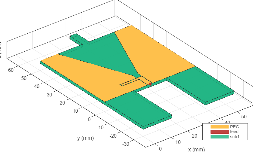
Analyze PCB Antenna
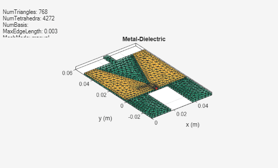
Mesh the antenna.
figure
mesh(p,MaxEdgeLength=3e-3,MinEdgeLength=2e-3);
Plot the S-parameters of the antenna.
freq = 0.05e9:0.1e9:6e9;
sp = sparameters(p,freq);
figure
rfplot(sp)
title("S11")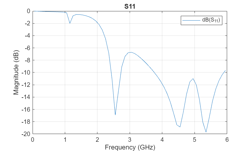
Reference
[1] Monebhurrun, Vikass, Satyajit Chakrabarti, and Richelieu Quoi. “A 5G NR FR1 UWB Antenna as Benchmark for the Development of IEEE Standard P2816.” In 2023 Antenna Measurement Techniques Association Symposium (AMTA), 1–2. Renton, WA, USA: IEEE, 2023. https://doi.org/10.23919/AMTA58553.2023.10293360.