Analysis of a Coplanar Strip Transmission Line with no Conductor Backing
This example demonstrates how to construct and feed a coplanar strip transmission line model using the RF PCB Toolbox's pcbComponent with feeds determined by FeedDefinition objects. The charactistic impedance of the line is calculated and compared against an analytical solution.
Introduction: Coplanar Strips
The coplanar strip transmission line consists of two parallel, coplanar traces. One trace is driven, and the other is grounded. Most notably, there is no metal ground plane or other metal grounding structure. The structure may lie on substrate; for simplicity, we omit this in the present setup.
Problem Setup
We aim to construct our device at 1 GHz and calculate the wavelength (lambda) accordingly.
freq = 1e9;
lightspeed = 299792458;
lambda = lightspeed/freq;
A coplanar strips problem can be specified in terms of the spacing a between the inner edges of the two traces and the spacing b between the outer edges of the two traces. From this information and a desired line length (electrically short for the impedance calculation), we can create two rectangles for the traces and start setting up a pcbComponent.
a = 0.5e-3;
b = 2.0e-3;
boardLength = lambda/20; % Electrically short - important for impedance calculation
boardWidth = b*5;

% Convert a and b into geometric information and create a rectangle for each strip
trace2CenterY = (a/2 + b/2)/2;
trace1CenterY = -trace2CenterY;
traceCenterX = boardLength/2;
traceWidth = (b-a)/2;

r1 = traceRectangular('Center', [traceCenterX trace1CenterY], 'Length', boardLength, 'Width', traceWidth);
r2 = traceRectangular('Center', [traceCenterX trace2CenterY], 'Length', boardLength, 'Width', traceWidth);

p = pcbComponent;
p.Layers = {r1 + r2};
p.BoardShape = traceRectangular('Length', boardLength, 'Width', boardWidth, 'Center', [boardLength/2 0]);
Next, we are to specify the pcbComponent object's feed. The standard method - setting the pcbComponent's FeedLocations property - is not viable in this case. The FeedLocations property can only be used to specify feeds that (a) span a single vertical gap on the board edge (cf. the microstripLine), (b) excite a via against a ground plane (cf. the Antenna Toolbox's Patch Antennas (Antenna Toolbox)), or (c) bisect and excite a contiguous metal region (cf. the Antenna Toolbox's slot (Antenna Toolbox)). In this case, we need to excite one location (the driven trace) against another location on the same layer (the ground trace) across a non-metallized gap.
To this end, we switch the pcbComponent's FeedFormat flag from "FeedLocations" to "FeedDefinitions" to directly edit the property FeedDefinitions. We instantiate and assign two FiniteGapFeed objects - one for each port - to apply excitation across a same-layer gap in the metal.
p.FeedFormat = 'FeedDefinitions';

% Feed 1: the near-end feed
f1 = FiniteGapFeed;
f1.SignalLocations = [0 trace1CenterY];
f1.GroundLocations = [0 trace2CenterY];
f1.SignalLayers = 1;
f1.SignalWidths = traceWidth;

% Feed 2: the far-end feed
f2 = copy(f1);
f2.SignalLocations(1,1) = boardLength;
f2.GroundLocations(1, 1) = boardLength;

% Assign the feeds to the pcbComponent
p.FeedDefinitions = [f1; f2];

figure; show(p)

Finally, we can mesh and solve the device.
figure; mesh(p, 'MaxEdgeLength', traceWidth);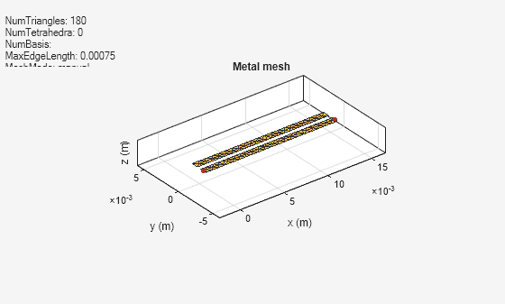
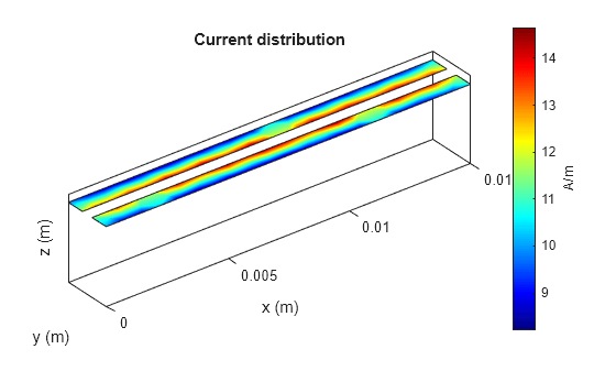
figure; current(p, freq);
sp1 = sparameters(p, freq);
To calculate the expected characteristic impedance, we use Eqs. (3.4.6.1), (3.4.6.3), (3.4.6.4), and (3.4.6.5) on p. 83 of [1]. Note that = 1 since no dielectric is present.
k = a/b;
kp = sqrt(1-k^2);
z0_expected = (120*pi) * ellipke(k)/ellipke(kp)
z0_expected =
203.1560
We then calculate the simulated characteristic impedance using a helper function coded at the end of this script.
z0_solver = calculateZ0(sp1)
z0_solver =
217.7038
The solver reports a characteristic impedance that is 14 ohms larger than expected. Manually reduce the mesh's minimum edge length and try again.
figure; mesh(p, 'MaxEdgeLength', traceWidth, 'MinEdgeLength', a/15);

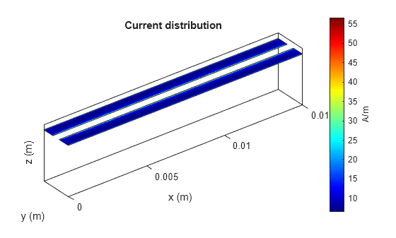
figure; current(p, freq);
sp2 = sparameters(p, freq);
z0_solver_corrected = calculateZ0(sp2)
z0_solver_corrected =
206.4504
The denser mesh reduces the impedance difference from 14 ohms to slightly more than 3 ohms. Compare the most recent current plot against the previous current plot; note that the denser mesh more accurately captures the large current densities at the inner edges of the coupled traces. This is a common result for edge-coupled structures solved by the Method of Moments: a very dense mesh is typically required at the coupled edges to obtain the expected behavior.
Helper function: calculateZ0
This helper function calculates the characteristic impedance from simulated S-parameters.
function z0 = calculateZ0(sp)
    s11 = sp.Parameters(1, 1, 1);
    s21 = sp.Parameters(2, 1, 1);
    zRef = sp.Impedance;
    zCal = ((1+s11).^2 - s21.^2)./((1-s11).^2 - s21.^2);
    z0 = abs(sqrt(zRef^2 * zCal));
end
References
[1] Wadell BC. Transmission Line Design Handbook. Norwood (MA): Artech House; 1991.