Model Coaxial Gap Feed for Probe-Fed Patch Antenna
This example shows the difference between a standard delta-gap probe feed model and a finite-gap coaxial feed model. It reproduces the input impedance results presented in Figure 3 of [1] using a patch antenna described in [2]. This example uses pcbComponent (RF PCB Toolbox) and pcbstack objects to create the patch antenna.
Usually, feeds on the pcbComponent object are defined using its FeedLocations property. While this workflow is fast and intuitive, it does not provide enough information to model feed structures that are more complex than basic probe feeds. Substituting a basic probe feed model for a more complex feed can cause substantial discrepancies in the antenna characteristics (S-parameters, impedance, and so on.) measured at the feed site. When you cannot adequately model a feed by using the FeedLocations property of the pcbComponent object, use its FeedDefinitions property instead and configure an appropriate feed from the FeedDefinitions (RF PCB Toolbox). This example shows that process using a scenario where the impedance behavior is strongly impacted by the choice of feed model.
Define Dimensions
The patch antenna used in this example is a 13.5-by-15 mm rectangular radiating element over a square ground plane. Figure 2 and Section III of [2] provide schematics, dimensions, and material properties for the patch antenna. Define the dimensions in meters, material properties, and analysis frequency range in hertz. In this example, the value for has been changed from 14 mm to 1.4 mm given the ground plane dimensions of 20-by-20 mm, as per the photograph in Figure 7 of [2], and the mesh shown in Figure 3 of [1]. The frequency limits in this example are chosen to match Figure 3 of [1].
Specify the top plate length and width in meters.
lp = 13.5e-3;
wp = 15.0e-3;
Specify the feed strip length and width in meters.
lm = 3.5e-3;
wm = 0.5e-3;
Specify the ground plane length and width in meters.
ls = 20e-3;
ws = 20e-3;
Specify the pad and antipad dimensions.
dOut= 1.0e-3;
dIn = 0.2e-3; % This comes from Sec. IIIA of [1].
sf  = 1.4e-3; % Deviation - original plan says 14 mm
Specify the substrate thickness in meters.
h = 0.8e-3;
Specify the relative permittivity and loss tangent of the dielectric material.
epsr = 4.4;
lossTang = 0.02;
Specify the analysis frequency range in hertz.
freq = linspace(4.5e9, 6e9, 61);
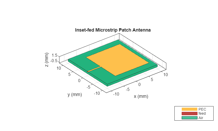
Edge-Fed Model for Inset-Fed Microstrip Patch Antenna
While it is possible to model this antenna using a pcbComponent object, the patchMicrostripInsetfed object straightforwardly constructs most of the geometry required. There are two caveats: first, the antenna is edge-fed instead of probe-fed, and second, you must add a very small notch where the feed trace touches the patch to satisfy the patchMicrostripInsetfed object's assumptions. Nevertheless, the patchMicrostripInsetfed object provides a good first estimate of the input impedance.
subm = dielectric(EpsilonR=epsr,LossTangent=lossTang,Thickness=h);
insetPatch = patchMicrostripInsetfed(Length=lp,Width=wp,Height=h,...
    GroundPlaneLength=ls,GroundPlaneWidth=ws,Substrate=subm,...
    StripLineWidth=wm,NotchLength=0.05e-3,NotchWidth=wm*2,...
    FeedOffset=[-(ls/2) 0],PatchCenterOffset=[-(ls/2 - sf - dOut/4 - lm - lp/2), 0]);
figure
show(insetPatch)
title("Inset-Fed Microstrip Patch Antenna");
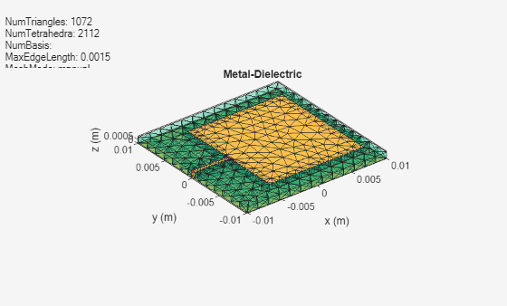
Mesh the antenna.
figure
mesh(insetPatch,MaxEdgeLength=1.5e-3,MinEdgeLength=1e-3);
Calculate the S-parameters of this antenna between 4.5 GHz to 6 GHz and convert them to Z-parameters.
s1 = sparameters(insetPatch,freq);
z1 = zparameters(s1);
Plot the impedance of this antenna using the plotZ helper function as defined in the Supporting Function section.
figure
plotZ(z1);
title("Input Impedance: Edge Feed");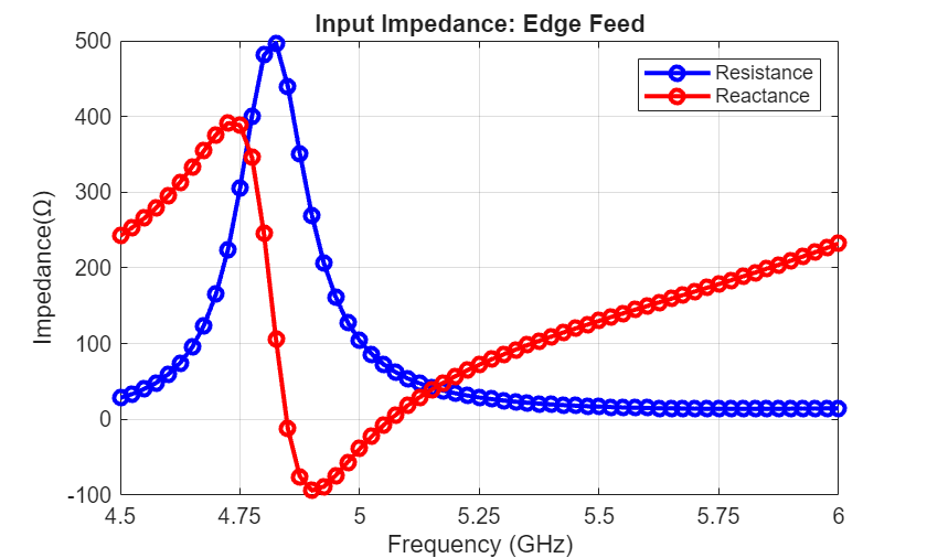
The edge feed model aligns well with the delta-gap curves in Figure 3 of [1], accurately capturing the maximum and minimum reactance values and the frequencies at which these features occur. However, the model deviates with respect to the maximum resistance.
Delta-Gap Probe Feed Model
To use a standard probe feed, convert the patchMicrostripInsetfed object to a pcbStack object, and then convert that pcbStack object to a pcbComponent object.
Copy the patch antenna's geometry to a pcbComponent object.
tempStack = pcbStack(insetPatch);
p = pcbComponent;
p.BoardThickness = tempStack.BoardThickness;
p.BoardShape = tempStack.BoardShape;
for j = 1:3
p.Layers{j} = copy(tempStack.Layers{j});
end
Warning: Dielectric thickness is updated with BoardThickness. Assign BoardThickness before setting up the Layers.
Cut the excess length out of the feed strip so that it only runs from the patch to the probe feed.
rectCut = traceRectangular(Length=(sf+dOut/4),Width=2*wm);
rectCut.Center = [-(ls - sf - dOut/4)/2 0];
p.Layers{1} = p.Layers{1} - rectCut;
Specify the feed location using the FeedLocations property and configure the other parameters of the feed. Calculate the probe feed location according to [2].
feedCenter = [-(ls/2 - sf - dOut/2), 0];
p.FeedLocations = [feedCenter 1 3];
p.FeedDiameter = dIn;
p.FeedViaModel = 'octagon';
figure
show(p)
Apply mesh to the antenna.
figure
mesh(p,MaxEdgeLength=1.5e-3,MinEdgeLength=1e-3);
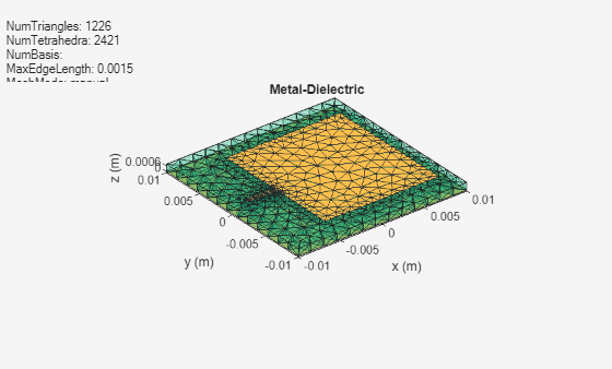
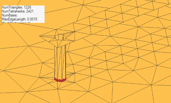
Zoom in on the feed.
figure
mesh(p,View="metal");
camdolly(-7.5e-3,0,0,'movetarget','data');
camzoom(20);
Now that the antenna is meshed, carry out the solution procedure for the delta-gap probe-fed antenna.
Calculate the S-parameters of this antenna between 4.5 GHz to 6 GHz and convert them to Z-parameters.
s2 = sparameters(p,freq);
z2 = zparameters(s2);
Plot the impedance of this antenna.
figure
plotZ(z2);
title("Input Impedance: Probe Feed");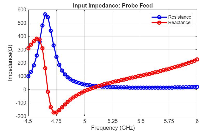
Compared against Figure 3 of [1], the impedance plot agrees with the Delta gap legend entries in these ways:
The resistance reaches nearly 600 ohms at its peak and declines rapidly to 0 ohms.
The reactance reaches nearly 400 ohms at its peak, swings to nearly –200 ohms, and then trends up towards 200 ohms.
However, the frequencies at which these features of the impedance plot occur are shifted by about 0.2 GHz relative to the reference.
Finite-Gap Coaxial Probe Feed Model
Replace the standard delta-gap probe feed by a finite-gap coaxial feed to better model the physics at the feed site.
Begin by adding a pad and antipad for the via.
Make sure that the pad and antipad:
(a) Are concentric
(b) Have the same number of edges
(c) Are not rotated relative to each other
numPadAntipadVertices = 8;
viaAntiPad = antenna.Circle(Radius=dOut/2,NumPoints=numPadAntipadVertices);
viaAntiPad.Center(1) = -(ls/2 - sf - dOut/2);

viaPad = antenna.Circle(Radius=dIn/2,NumPoints=numPadAntipadVertices);
viaPad.Center(1) = -(ls/2 - sf - dOut/2);
Punch out the antipad from the ground plane and add back in the pad. Note that, the order of operations matters.
p.Layers{3} = p.Layers{3} - viaAntiPad + viaPad;The pcbComponent object cannot automatically recognize a coaxial feed based on its FeedLocations property. For this reason, specify the FeedDefinitions property using a CoaxialFeed object.
To enable the FeedDefinitions property, specify the FeedFormat property as 'FeedDefinitions'. This disables the FeedLocations property and the pcbComponent object automatically converts any feed information specified previously using the FeedLocations property to a ProbeFeed feed definition object.
p.FeedFormat = 'FeedDefinitions'p =
pcbComponent with properties:
Name: 'MyPCB'
Revision: 'v1.0'
BoardShape: [1×1 antenna.Rectangle]
BoardThickness: 8.0000e-04
Layers: {[1×1 antenna.Polygon] [1×1 dielectric] [1×1 antenna.Polygon]}
FeedFormat: 'FeedDefinitions'
FeedDefinitions: [1×1 ProbeFeed]
ViaLocations: []
ViaDiameter: []
FeedViaModel: 'octagon'
Conductor: [1×1 metal]
Tilt: 0
TiltAxis: [0 0 1]
Load: [1×1 lumpedElement]
Create a CoaxialFeed object to replace the previous ProbeFeed object.
f1 = CoaxialFeed;
f1.PadShape = viaPad;
f1.AntipadShape = viaAntiPad;
f1.SignalLayers = 1;
f1.GroundLayers = 3;
Assign the CoaxialFeed object to the FeedDefinitions property of the pcbComponent object.
p.FeedDefinitions = f1;
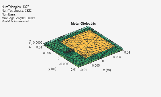
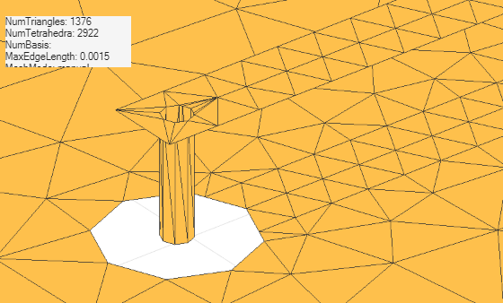
After assigning the CoaxialFeed object to the FeedDefinitions property, view the new mesh and feed site.
figure
mesh(p,MaxEdgeLength=1.5e-3,MinEdgeLength=1e-3);
Zoom in on the feed.
figure
mesh(p,View="metal");
camdolly(-7.5e-3,0,0,'movetarget','data');
camzoom(20);
Calculate the S-parameters and convert them to Z-parameters.
s3 = sparameters(p, freq);
z3 = zparameters(s3);
Plot the impedance.
figure
plotZ(z3);
title("Input Impedance: Coaxial Feed")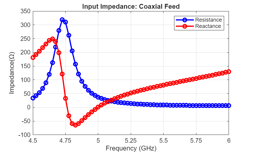
Similar to probe-fed impedance, the impedance curves here are very close to the curves labeled Proposed in Figure 3 of [1] in terms of feature magnitudes, but they deviate by roughly 0.2 GHz in terms of feature locations.
Conclusion
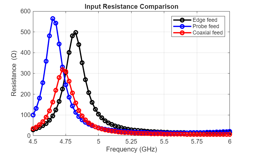
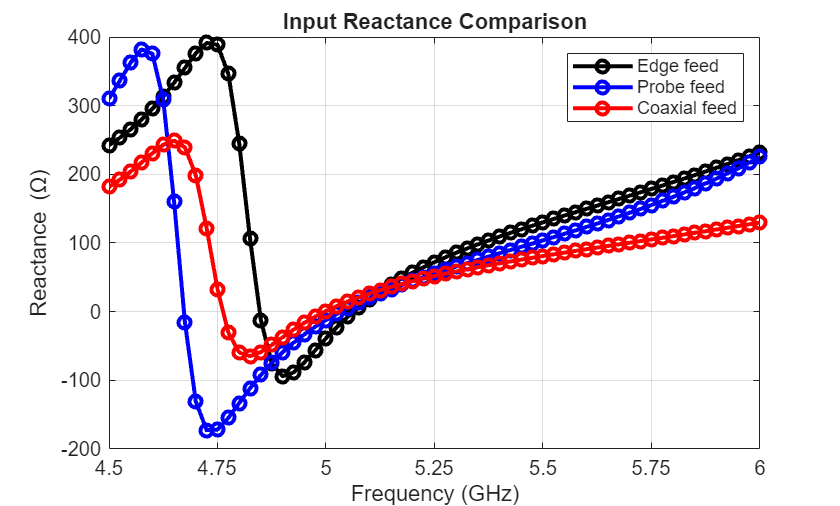
In this example, you simulate a probe-fed patch antenna with three different feed models: a standard edge feed, a standard delta-gap probe feed specified using the FeedLocations property, and a more realistic finite-gap coaxial feed specified using the FeedDefinitions property of the pcbComponent object. Changing the feed from a probe feed to a coaxial feed changes the maximum resistance and reactance by roughly 42% and 37%, respectively. The simulated results for both feeds are validated because they closely match the results in [1], except for a frequency shift of 3-4% (0.125 GHz relative to 6 GHz and 4.5 GHz, respectively) relative to the results reported in [1].
These figures compare resistance and reactance for the three types of feed. The input impedance of the coaxial feed substantially decreases relative to the edge and probe feeds in all cases.
zp1 = squeeze(z1.Parameters);
zp2 = squeeze(z2.Parameters);
zp3 = squeeze(z3.Parameters);
Compare the resistance.
figure
plot(freq/1e9,real(zp1),'-ok',LineWidth=2);
hold on;
plot(freq/1e9,real(zp2),'-ob',LineWidth=2);
plot(freq/1e9,real(zp3),'-or',LineWidth=2);
xticks(min(freq)/1e9:0.25:max(freq)/1e9);
ylim([0 600]);
grid on;
legend({"Edge feed", "Probe feed", "Coaxial feed"});
xlabel("Frequency (GHz)");
ylabel("Resistance (\Omega)");
title("Input Resistance Comparison");
Compare the reactance.
figure
plot(freq/1e9,imag(zp1),'-ok',LineWidth=2);
hold on;
plot(freq/1e9,imag(zp2),'-ob',LineWidth=2);
plot(freq/1e9,imag(zp3),'-or',LineWidth=2);
xticks(min(freq)/1e9:0.25:max(freq)/1e9);
ylim([-200 400]);
grid on;
legend({"Edge feed", "Probe feed", "Coaxial feed"});
xlabel("Frequency (GHz)");
ylabel("Reactance (\Omega)");
title("Input Reactance Comparison");
Supporting Function
This helper function plots the impedance curves and is used throughout the example for that purpose.
function plotZ(zp)
    zp2 = squeeze(zp.Parameters);
    freq = zp.Frequencies;
    plot(freq/1e9, real(zp2),'-ob',LineWidth=2);
    hold on;
    plot(freq/1e9, imag(zp2),'-or',LineWidth=2);

    xticks(min(freq)/1e9: 0.25:max(freq)/1e9);
    legend({"Resistance", "Reactance"});
    xlabel("Frequency (GHz)");
    ylabel("Impedance(\Omega)");
    grid on;
end
References
[1] Liu, Chang, and Ali E. Yilmaz. “A Generalized Finite-Gap Lumped-Port Model.” In 2018 IEEE 27th Conference on Electrical Performance of Electronic Packaging and Systems (EPEPS), 173–75. San Jose, CA: IEEE, 2018. https://doi.org/10.1109/EPEPS.2018.8534282.
[2] Li Li, Xinwei Chen, Yi Zhang, Liping Han, and Wenmei Zhang. “Modeling and Design of Microstrip Patch Antenna-in-Package for Integrating the RFIC in the Inner Cavity.” IEEE Antennas and Wireless Propagation Letters 13 (2014): 559–62. https://doi.org/10.1109/LAWP.2014.2312420.
See Also
Objects
pcbComponent(RF PCB Toolbox) |pcbStack|patchMicrostripInsetfed|antenna.Circle
Functions
mesh|sparameters|zparameters(RF Toolbox)