Design, Analyze, and Optimize H-Notch Patch Using Design Variables
This tutorial shows how to define the metal patch, dielectric, and ground plane layers in H-notch patch antenna using design variables in the PCB Antenna Designer app and optimize the design for maximum gain.
Open New Session
Type this command at the command line to open the PCB Antenna Designer app.
pcbAntennaDesigner
On the Design tab, click New Session to start a new session and open a blank canvas.
Define Board Shape
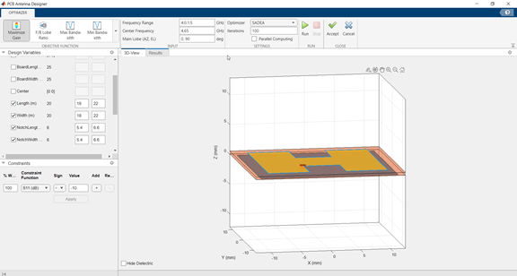
To design a PCB stack, you must first define a board shape. Select Rectangle from the Shapes section on the toolbar. Drag the shape on the canvas to create a rectangle.
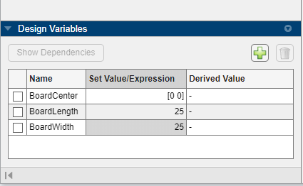
Use the Design Variables tab to add variables for the board center, board length, and board width. To add a new variable, click ![]() . Add the following to the table:
. Add the following to the table:
BoardCenter —
[0,0]BoardLength —
25BoardWidth —
25
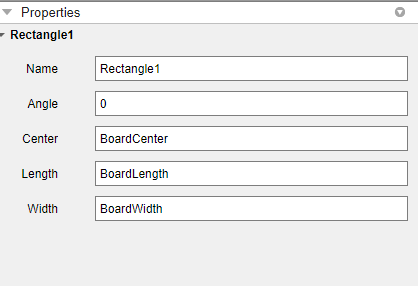
Add the variables to the Rectangle1 properties tab.
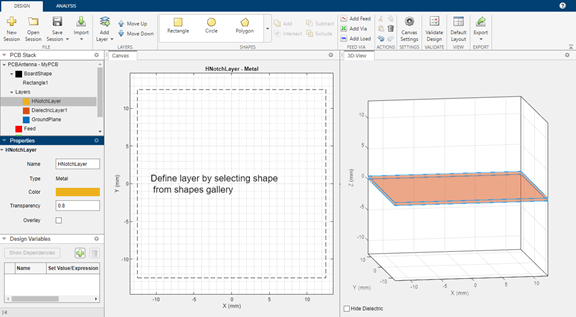
Add Ground, Metal, and Dielectric Layer
Click Add Layer on the toolbar and then select Metal Layer to add a metal layer.
Set the Name of the metal layer to GroundPlane.
Click Add Layer on the toolbar and then select Dielectric Layer to add a dielectric layer DielectricLayer1.
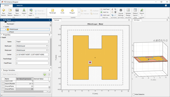
Click Add Layer on the toolbar and then select Metal Layer to add a metal layer. Set the name of this layer to HNotchLayer.
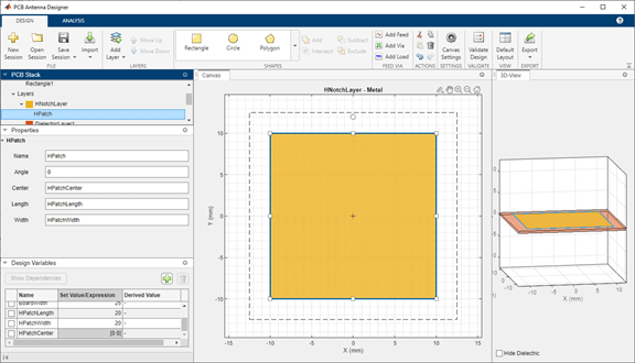
Create H-Notch
Select the HNotchLayer on the PCB Stack navigation tree and then select Rectangle from the Shapes section on the toolbar. Drag the shape onto the canvas to create a rectangular patch.
Use the Design Variables tab to set the properties of the HPatch.
Center —
[0,0]Length —
20Width —
20
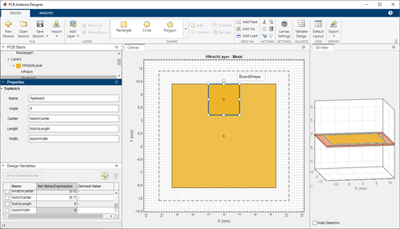
Create Top Notch
Select Rectangle from the Shapes section and drag the shape to the top of the shape to create a top notch in the patch layer. Set the properties of Rectangle3 to the following using the Design Variable tab.
Name —
TopNotchCenter —
[0,7]Length —
6Width —
6
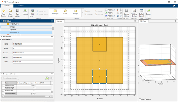
Create Bottom Notch
Select TopNotch from the canvas and then copy the layer by clicking Copy in the Actions section. Click Paste to paste a copy of TopNotch. Doing so creates a rectangle TopNotch_Copy_1 with identical dimensions to the TopNotch layer.
Set the properties of TopNotch_Copy_1 to the following:
Name —
BottomNotchCenter —
[0,-7]
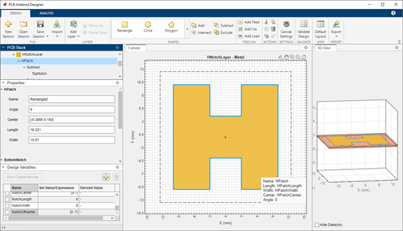
Subtract Top and Bottom Notch Layers from Metal Patch
Select HPatch and TopNotch and then click Subtract in the Shapes section of the toolbar to remove both rectangles.
Select the HPatch and BottomNotch and click Subtract in the Shapes section of the toolbar to remove both rectangles.
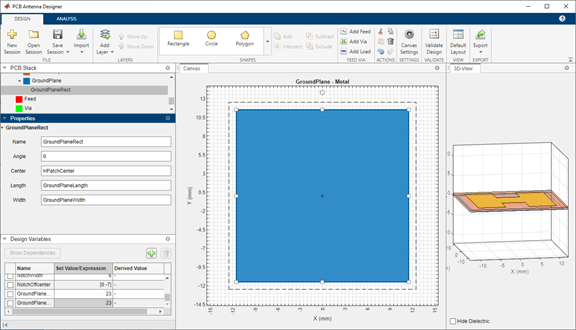
Set Dimensions for Ground Plane
The ground plane must be same size as the HNotchLayer. To make the ground plane the same size as HPatch, right-click HPatch and select Copy.
Right-click the GroundPlane and click Paste on the toolbar to paste the rectangle in the GroundPlane.
The app copies the rectangle to the ground plane layer with the name HPatch_Copy(1). HPatch_Copy(1) and HPatch have the same dimensions.
Set the properties of HPatch_Copy(1) to the following:
Name —
GroundPlaneRectCenter —
[0,0]Length —
23Width —
23
Add Feed
Select the HNotchLayer metal layer on the PCB Stack navigation tree and then click Add Feed in the Feed Via section on the toolbar. You can add a feed only to a metal layer.
As the PCB Stack navigation tree shows, the app adds the feed to HNotchLayer as Feed1.
Select the parent Feed node on the PCB Stack navigation tree, and then set the FeedDiameter to 1 and FeedViaModel to Strip. FeedDiameter is a global property.
Change Position of Feed
Select Feed1 on the PCB Stack navigation tree. In the Properties pane, set Center to [-3,-3].
In the 3D-View pane, you can see that the feed is connected only to HNotchLayer.

For more information on feeds and vias, refer to the FeedLocation and ViaLocation property descriptions in the pcbStack object documentation.
Change Start Layer and Stop Layer
Connect the feed from HNotchLayer to GroundPlane by setting StartLayer to HNotchLayer and StopLayer to GroundPlane. This creates a feed on the GroundPlane which connects to the HNotchLayer.
Change Metal Properties
Select the Layers in on the PCB Stack navigation tree and set the Type of the metal layer to Copper in the Properties pane.
Validate Design
Click Validate Design on the toolbar to validate your board shape, layers, feed, via, and load.
Analyze H-Notch Unit Element
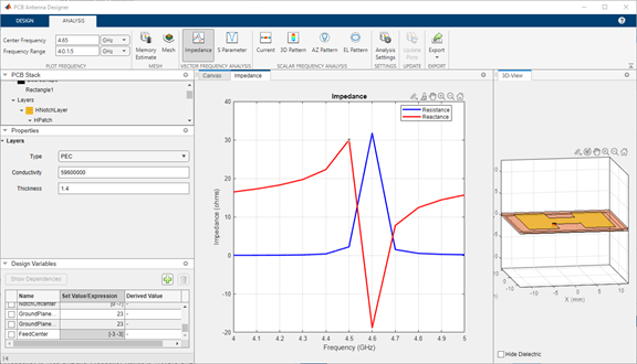
In the Analysis tab, set the Center Frequency to 4.65 GHz and Frequency Range to 4:0.1:5 GHz
Run Analysis
Select Impedance from the Vector Frequency Analysis section on the toolbar to plot the impedance plot. The impedance plot shows that the PCB stack antenna resonates at 4.6 GHz.
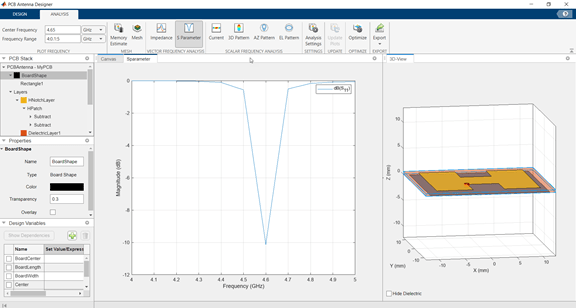
Select S Parameter from the Vector Frequency Analysis section on the toolbar to plot the S11.
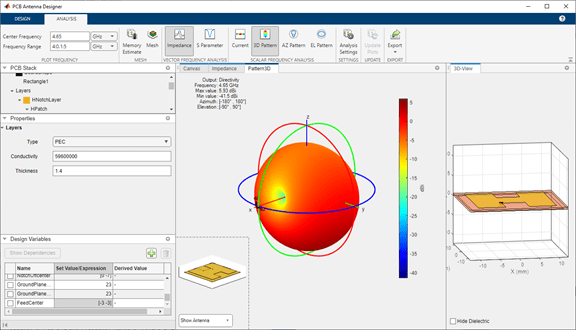
Click 3D Pattern from the Scalar Frequency Analysis section on the toolbar to plot the 3-D far-field radiation pattern of the antenna. The directivity of the H-notch patch unit element is 5.93 dBi.
Setup Optimization Problem
Any optimization problem typically requires following inputs.
Objective function: Main goal of the optimization. It evaluates the analysis function and minimizes or maximizes the output of the function. In this tutorial, maximizing the gain of the antenna is the objective function.
Design variables: The input variables to the objective function. These variables are changed by the optimizer within a pre-set range of values called as the bounds of the variables. In this tutorial, the dimensions of the H-Notch patch are the design variables.
Constraint functions (if necessary): Functions which restrict a desired analysis function value on the antenna. In this tutorial, the constraint function is S11 less than -10 db to obtain an impedance bandwidth.
Other inputs: Other inputs may include the number of iterations, the input center frequency, and the input frequency, the frequency at which the analysis is performed, etc.
Optimization Function, Design Variables, and Constraints
To optimize the H-Notch patch, click on the Optimize button. To select an objective function, use the OBJECTIVE FUNCTION Gallery drop down. Since the goal is to maximize the gain of the antenna, click on Maximize Gain. To set up the design variables, click on the Design Variables tab. Click on the checkboxes present on the left-hand side of the properties to choose the required design variables. The optimizer would change these chosen properties to obtain a maximum gain for the antenna. To set up the constraints, click on the Constraints tab and select S11 (dB) from the Constraint Function. Select < operator from sign and enter value as -10.
Click Apply.
In the SETTINGS section, enter the number of Iterations to run for the optimizer. To start the optimization, click the Run button.
Optimization
The SADEA optimization contains two stages:
Building model
Optimizing
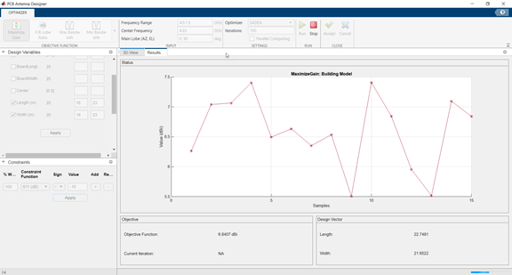
Building Model
In the model building stage, the optimizer makes a surrogate model from the design space, and the specified objective and the constraints function. It diversely goes through the design space and performs analysis on these sample points.
So, the X-axis shows the number of samples and the Y-axis shows the value of the analysis function value at that sample. The bottom left side show the current sample value and the bottom right side shows the design variables. The optimizer within decides and takes appropriate number of samples to build the model. After the model is built, the optimizer starts running iterations.
Optimizing
In the optimizing stage, the X-axis shows the number of iterations and the Y-axis shows the objective function values. From the plots shown on the optimizing stage, you can understand the trend of convergence.
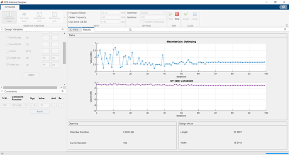
Once the optimization is complete, click on Accept. This takes you back to the Analysis tab. And the dimensions are updated with the optimized values. Run the Impedance, S Parameters, and 3D Pattern analysis again to compare optimization results with the original results.
See Also
Objects
Functions
subtract|impedance|sparameters|pattern