Main Content

Push-Pull Output

Behavioral representation of CMOS complementary output stage

  • Push-Pull Output block

Libraries:
Simscape / Electrical / Integrated Circuits

Description

The Push-Pull Output block represents a CMOS complementary output stage behaviorally. To improve simulation speed, the block does not model all the internal individual MOSFET devices that make up the gate. You can use this block to create a representative output current-voltage relationship when defining an integrated circuit model behavior with Physical Signal blocks from the Simscape™ Foundation library.

You can choose between are two output current-voltage relationships:

  • Linear — The block represents the output as a voltage source plus series resistance and parallel capacitance, as shown in the following figure. The value you specify for the Output resistance parameter is assigned to the series resistance, and the capacitance values are determined by matching the RC time constant to the Propagation delay parameter value.
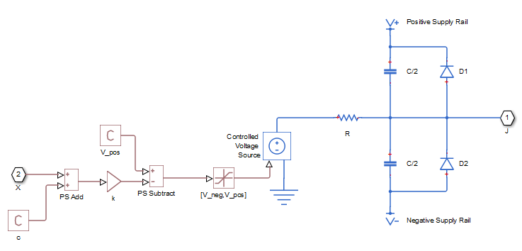
    The input to the Controlled Voltage Source block is limited to be between the supply rails, and it is also inverted by subtraction from the supply voltage. The inversion makes it behave like a complementary output stage, with a high gate-source voltage resulting in a low output.

  • Quadratic — The output stage is modeled by the two MOSFETs that constitute the complementary pair. The MOSFET parameters are derived from the output resistance values and short-circuit currents that you specify as mask parameters. The gate input demand is lagged to approximate the Propagation delay parameter value.
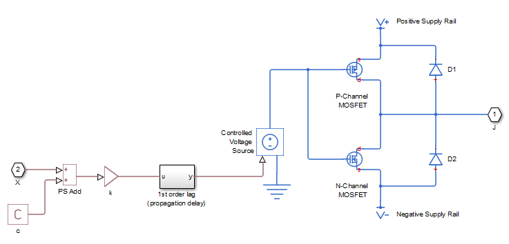
Both Linear and Quadratic output models add an offset and scale the physical input X so that the gate voltage is given by:

Vg = k · ( X + c )(1)

where

  • k is the input signal scaling.

  • c is the input signal offset.

The offset and scaling can be used, for example, to match logical values for X (that is, range [0,1] ) to [V-, V+] at the output pin. For example, if V+ = 10V and V- = 0, then to match the signal logical values to this voltage range, set c = -1 and k = -10.

For both Linear and Quadratic output models, the protection diodes D1 and D2 act to limit the output voltage range. These diodes are Diode blocks from the Simscape Foundation library, that is, piecewise linear diodes defined by their forward voltage and on resistance. If the voltage across D1 rises above the forward voltage, then the diode starts to conduct, and provided that the on resistance is low, it effectively prevents the output rising above V+ plus the diode forward voltage drop. An equivalent behavior results if the output voltage drops too low.

The output model is very similar to that used for the logic blocks. For a plot of a typical output V-I characteristic when using the Quadratic output model, see Selecting the Output Model for Logic Blocks.

Note

This block is constructed out of blocks from the Simscape Physical Signals library (such as PS Add, PS Gain, and so on). Currently, the blocks in the Physical Signals library do not support unit propagation and checking. For more information, see How to Work with Physical Units.

Examples

Assumptions and Limitations

  • The block does not accurately model dynamic response.

  • The Quadratic output model does not model any output capacitance effects. Add output capacitance externally to the block if required.

Ports

Input

expand all

Physical port associated with the Push-Pull Output input.

Conserving

expand all

Electrical conserving port associated with the block output. The port name is hidden on the block icon, but you can see it in simulation data logs.

Parameters

expand all

Input Scaling

The input physical signal X is mapped to the gate voltage by Vg = k · ( X + c ), where k is the input signal scaling. Use this parameter in conjunction with the Input signal offset, c to map the range of X to the voltage range defined by the power supply.

The input physical signal X is mapped to the gate voltage by Vg = k · ( X + c ), where c is the input signal offset. Use this parameter in conjunction with the Input signal scaling, k to map the range of X to the voltage range defined by the power supply.

Output Characteristics

Select the output model:

  • Linear - the output voltage drops linearly with output current. This is the default option.

  • Quadratic - the output voltage dependency on output current is defined by the quadratic I-V characteristics of the two output MOSFET devices.

Defines one over the slope of the output I-V characteristic.

Dependencies

This parameter is visible only when the Output current-voltage relationship parameter is set to Linear.

Defines the rail voltages for which mask data output resistances and currents are defined.

Dependencies

This parameter is visible only when the Output current-voltage relationship parameter is set to Quadratic.

A row vector [ R_OH1 R_OH2 ] of two resistance values. The first value R_OH1 is the gradient of the output voltage-current relationship when the complementary pair output is HIGH (Vg=V-) and there is no output current. The second value R_OH2 is the gradient of the output voltage-current relationship when the output is HIGH and the output current is I_OH.

Dependencies

This parameter is visible only when the Output current-voltage relationship parameter is set to Quadratic.

The resulting current when the output is HIGH (Vg=V-), but the load forces the output voltage to the negative supply rail.

Dependencies

This parameter is visible only when the Output current-voltage relationship parameter is set to Quadratic.

A row vector [ R_OL1 R_OL2 ] of two resistance values. The first value R_OL1 is the gradient of the output voltage-current relationship when the complementary pair output is LOW (Vg=V+) and there is no output current. The second value R_OL2 is the gradient of the output voltage-current relationship when the output is LOW and the output current is I_OL.

Dependencies

This parameter is visible only when the Output current-voltage relationship parameter is set to Quadratic.

The resulting current when the output is LOW (Vg=V+), but the load forces the output voltage to the positive supply voltage.

Dependencies

This parameter is visible only when the Output current-voltage relationship parameter is set to Quadratic.

Time it takes for the output to reach 63.2% of its final value following a step change in the input, X. For Quadratic output, it is implemented by the lagged gate input demand.

The gradient of the voltage-current relationship for the protection diodes when forward biased.

The voltage above which the protection diode is turned on.

Supply Voltage

Negative power supply voltage applied to the N-channel MOSFET source pin.

Positive power supply voltage applied to the P-channel MOSFET source pin.

Initial Conditions

This parameter is used to set the voltage on the output capacitors so that the output voltage is initialized to the parameter’s value.

Dependencies

This parameter is visible only when the Output current-voltage relationship parameter is set to Linear on the Output Characteristics tab.

This parameter is used to initialize the propagation delay first-order lag such that there is no transient at time zero.

Dependencies

This parameter is visible only when the Output current-voltage relationship parameter is set to Quadratic on the Output Characteristics tab.

Extended Capabilities

C/C++ Code Generation
Generate C and C++ code using Simulink® Coder™.

Version History

Introduced in R2011b