Validate RF Data Converter Configuration
This example shows how to validate an RF data converter (RFDC) configuration in a simulation. An RFDC has several interdependent parameters that you can configure. Fine-tuning these parameters is difficult when the design runs on hardware. In this example, you simulate the RF Data Converter block with two different configurations. One configuration shows the response of a tone and the other shows the response of a 5G NR FR1 waveform. You can also observe the RFDC configuration effects and modify the RFDC configuration to receive and transmit the waveform without any distortion.
Introduction
In wireless communication systems, designing the transmit and receive chains with the direct RF sampling data converters is a challenge. In RF transceivers, the transmit path consists of the interpolation filters, a complex mixer, and a digital to analog converter (DAC). The receive path consists of an analog to digital converter (ADC), a complex mixer, and the decimation filters. In RFSoC devices, the interpolation and decimation filters, complex mixers, ADC, and DAC are integrated inside the chip as part of the RFDC. This block diagram shows the typical transmit and receive paths.
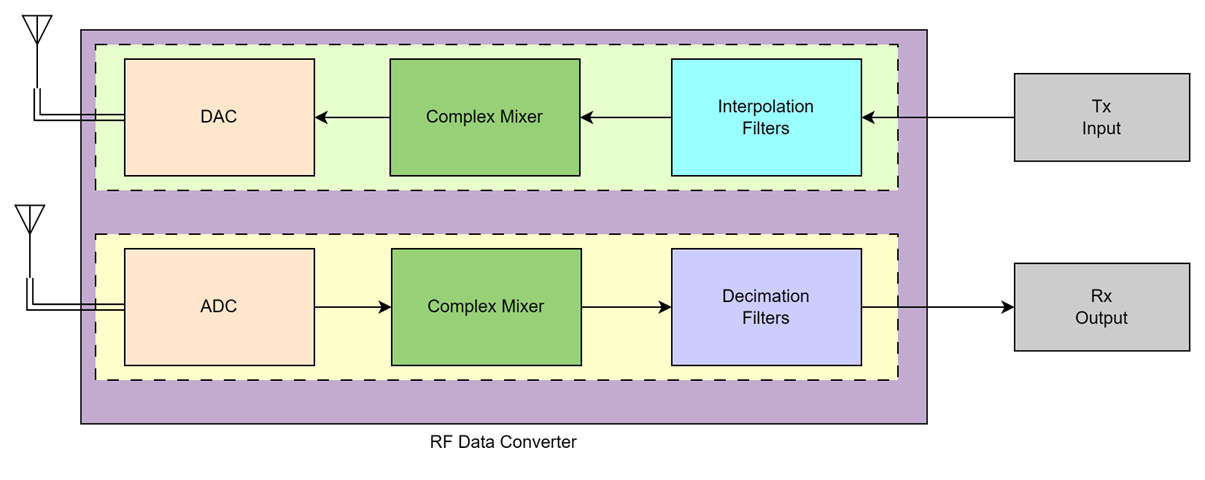
Interpolation filters upsample the input signal by an integer-valued factor. The decimation filters downsample the input signal by an integer-valued factor. A complex mixer shifts the input signal frequency spectrum to center it around the provided carrier frequency (Fc). When you choose a carrier frequency that is less than half of the sampling rate (Fs), the original signal shifts such that it is centered around the provided carrier frequency.

In another scenario, when you choose a carrier frequency Fc that is greater than half of the sampling rate Fs, the RF Data Converter block calculates the effective frequency (effNCOFreq) for zone 1 and shifts the image of original signal to center it around the provided carrier frequency.

To simulate the interpolation and decimation filters and complex mixers, select Behavioral mode in the RF Data Converter block mask, as this figure shows.

For more information about RF Data Converter block parameters, see RF Data Converter.
Simulation with Sinusoidal Waveform
open_system('rfdcSim_tone')

close_system('rfdcSim_tone')
Model setup:
The model consists of an RF Data Converter block configured with behavioral simulation mode and an NCO block to generate the complex sinusoidal signal. In the RFDC block, in the DAC tab, select DAC 0 in Tile 0. In the ADC tab, select ADC 0 in Tile 0. The output of the NCO block connects to the I and Q ports of DAC 0 (dacT0Ch0IData and dacT0Ch0QData, respectively) through the Complex to Real-Imag block. The dacT0Ch0 output of the DAC connects as an input to the ADC (adcT0Ch0) through the RF Channel subsystem. The RF Channel subsystem adds white Gaussian noise to the output of the DAC. The output of the RF Channel subsystem connects to the RF spectrum analyzer block, where you can visualize the frequency spectrum of the DAC output signal. The adcT0Ch0IData and adcT0Ch0QData outputs of the ADC connect to the RX spectrum analyzer block through the Real-Imag to Complex block. You can visualize the frequency spectrum of the input signal in the TX spectrum analyzer.
The RF Data Converter block has these parameter values:
Digital interface as
I/QSampling rate (MSPS) as
2048Interpolation mode (xN) and Decimation mode (xN) as
4NCO frequency (GHz) as
0.6
The input signal has these characteristics:
Frequency of 64 MHz
Sampling rate of 512 MSPS

Open the model by running this command.
open_system('rfdcSim_tone');
Run the simulation. Observe that in the RF spectrum analyzer block, the RFDC upsamples the input signal by the provided interpolation factor at the DAC output. The RFDC shifts the input signal by the provided NCO frequency at the DAC output.
Observe that in the Rx spectrum analyzer block, the RFDC shifts the received signal by the provided NCO frequency at the ADC output. The RFDC downsamples the received signal by the provided decimation factor at ADC output.
This figure shows the spectrum of the transmitted waveform at the DAC input.

This figure shows the spectrum of the transmitted waveform at the DAC output.

This figure shows the spectrum of the received waveform at the ADC output.

You can also run the simulation by specifying different parameters in the RFDC block or changing the input signal.
Simulation with 5G Waveform
open_system('rfdcSim_5G')

close_system('rfdcSim_5G')
Model setup:
The model consists of an RF Data Converter block configured with behavioral simulation mode and a Signal From Workspace block to output the 5G waveform. This model uses a 5G NR FR1 waveform that was generated using the Wireless Waveform Generator app as an input to the RFDC block. In the RF Data Converter block, in the DAC tab, select DAC 0 in Tile 0. In the ADC tab, select ADC 0 in Tile 0. The output of the NCO block connects to the I and Q ports of DAC 0 (dacT0Ch0IData and dacT0Ch0QData, respectively) through the Complex to Real-Imag block. The dacT0Ch0 output of the DAC connects as an input to the ADC (adcT0Ch0) through the RF Channel subsystem. The RF Channel subsystem adds white Gaussian noise to the output of the DAC. The output of the RF Channel subsystem connects to the RF spectrum analyzer block, where you can visualize the frequency spectrum of the DAC output signal. The adcT0Ch0IData and adcT0Ch0QData outputs of the ADC connect to the Rx spectrum analyzer block through the Real-Imag to Complex block. You can visualize the frequency spectrum of the input signal in the Tx spectrum analyzer.
The RF Data Converter block has these parameter values:
Digital interface as
I/QSample rate (MSPS) as
1024Interpolation mode (xN) and Decimation mode (xN) as
2NCO frequency (GHz) as
0.35
The input signal has these characteristics:
5G NR FR1 waveform that was generated using the Wireless Waveform Generator app
Bandwidth of 100 MHz
Sampling rate of 512 MSPS

Open the model by running this command.
open_system('rfdcSim_5G');
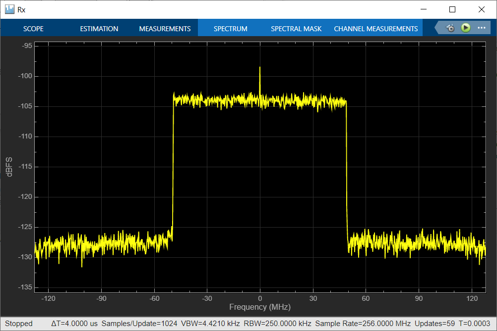
Run the simulation. Observe that you receive some unwanted frequency bands in the Tx spectrum analyzer block.
This figure shows the spectrum of the transmitted waveform at the ADC input.

This figure shows the spectrum of the transmitted waveform at the DAC output and the ADC input.

This figure shows the spectrum of the received waveform at the ADC output.

To avoid the unwanted frequency bands in the receiver spectrum, select higher interpolation and decimation modes. Specify Interpolation mode (xN) as 4 and Decimation mode (xN) as 4. The updated input signal sampling rate is 256 MSPS.
Run the simulation again after updating the parameters. By increasing the interpolation and decimation modes, you eliminate the unwanted frequency bands in the spectrum of the received waveform, as this figure shows.
Try Different Hardware Boards
The hardware board in the above two models is set to Xilinx Zynq UltraScale+ RFSoC ZCU111 Evaluation Kit, which is a Gen 1-based RFSoC device. To switch to a different RFSoC board, on the System on Chip tab, set Hardware Board to either Xilinx Zynq UltraScale+ RFSoC ZCU208 Evaluation Kit or Xilinx Zynq UltraScale+ RFSoC ZCU216 Evaluation Kit, which are Gen 3-based RFSoC devices.
The RFDC specifications vary across different RFSoC generations. For example, the available interpolation modes for Gen 1 and Gen 2 RFSoC devices are 1, 2, 4, and 8, whereas the available interpolation modes for Gen 3 RFSoC devices are 1, 2, 3, 4, 5, 6, 8, 10, 12, 16, 20, 24, and 40.
Summary
This example shows how to validate an RFDC configuration using a simulation. Using this example as a reference, you can design and validate your RF configurations for different RFSoC devices.