Receive Tone with DDR4 Using IP Core Generation Workflow on Xilinx RFSoC Device
This example shows how to design, simulate, and deploy an algorithm to write and read the captured RF samples from external double data rate 4 (DDR4) memory in Simulink® targeted on the Xilinx® Zynq™ UltraScale+™ RFSoC ZCU111 evaluation kit. In this example, you can write the captured samples of an analog-to-digital converter (ADC) into external programmable logic (PL) DDR4 memory, read the samples from the PL DDR4 memory, and send them to the host to display. A tone signal is generated in FPGA using a numerically controlled oscillator (NCO) to verify the receive path.
Supported Hardware Platforms
Xilinx Zynq UltraScale+ RFSoC ZCU111 Evaluation Kit + XM500 balun card
Design Task and System Specifications
Consider an RF application that requires accessing external DDR4 memory to capture RF samples at a high data rate. In this example, the design task is to design a control algorithm that writes and reads captured RF samples from the external PL DDR4 memory. To verify RF samples captured on the DDR4, send a sinusoid tone from the FPGA to the digital-to-analog converter (DAC) of the RF Data Converter block (output of the DAC is looped back to the ADC input), and receive the data back to the FPGA. The following are the system specifications.
System Specifications
ADC and DAC sampling rate = 2048 MSPS
Number of ADC channels = 1
Number of DAC channels = 1
Digital data interface = Real
Model Structure
On the top level, this example model consists of RF Data Converter and AXI4 Random Access Memory blocks and Transmit and Receive Tone subsystem. On the transmit side, in Transmit and Receive Tone subsystem, the NCO subsystem, which connects to the DAC in RF Data Converter block, generates four consecutive samples of the sinusoid waveform by using the NCO block. Each sample has a word length of 16-bits. You can use the input port NCO_PhaseIncrement to adjust the frequency of the sinusoid waveform.
In the RF Data Converter block, the DAC interpolates the input data by a factor provided in the block mask. The output of the DAC is loop back to the ADC in RF Data Converter block. The ADC decimates the input data by a factor provided in the block mask. The ADC in RF Data Converter block connects to the receive side of the Transmit and Receive Tone subsystem.
On the receive side, in Transmit and Receive Tone subsystem, the DDR Capture Logic subsystem writes the received data to PL DDR. You can use the input port FrameSize to specify the size of the data to read from and write to PL DDR. After the DDR Capture Logic subsystem writes the required amount of data to PL DDR, then it starts reading the data from PL DDR. Then, the subsystem streams the data back to the host for further processing or display.
This example is configured with Real ADC/DAC Interface reference design to run on Xilinx Zynq UltraScale+ RFSoC ZCU111 Evaluation Kit.
open_system('soc_datacapture_ddr')

close_system('soc_datacapture_ddr')
Simulation
Simulate the model and observe the spectrums in all spectrum analyzer blocks. The Random Access Memory block helps to verify the DDR read or write logic in the Transmit and Receive Tone subsystem. This block also provides the information related to memory performance such as throughput, latency. See block help page to know more about the memory diagnostics.
You can observe that the sample rate of sinusoid in RF spectrum analyzer block is 2048 MHz, which is due to the interpolation of the DAC in RF Data Converter block. You can also observe that the sample rate of the sinusoid in Rx spectrum analyzer block is 512 MHz, which is due to the decimation of the ADC in RF Data Converter block.
Transmit waveform

RF waveform

Receive waveform

To visualize the memory performance, after running the simulation, open the performance report by following these steps.
On the System on Chip toolstrip tab, click Performance Report.
In the Performance Report window that opens, in the Report Browser pane, select PL Memory Controller.
In the Controls pane, set Select plot type to
Bandwidth. Select Master 1 Write and Master 2 Read.Click Create Plot to display the bandwidth usage of the PL memory controller.

Implementation
Hardware Setup for ZCU111 Kit
Connect the SMA connectors on the XM500 balun card to complete the loopback between the DACs and ADCs, according to the connections provided in the following table.

To implement the model on a supported SoC board, use the HDL Coder™ IP core generation workflow. To add the HDL Code tab to the Simulink toolstrip, open the Apps gallery and select HDL Coder.
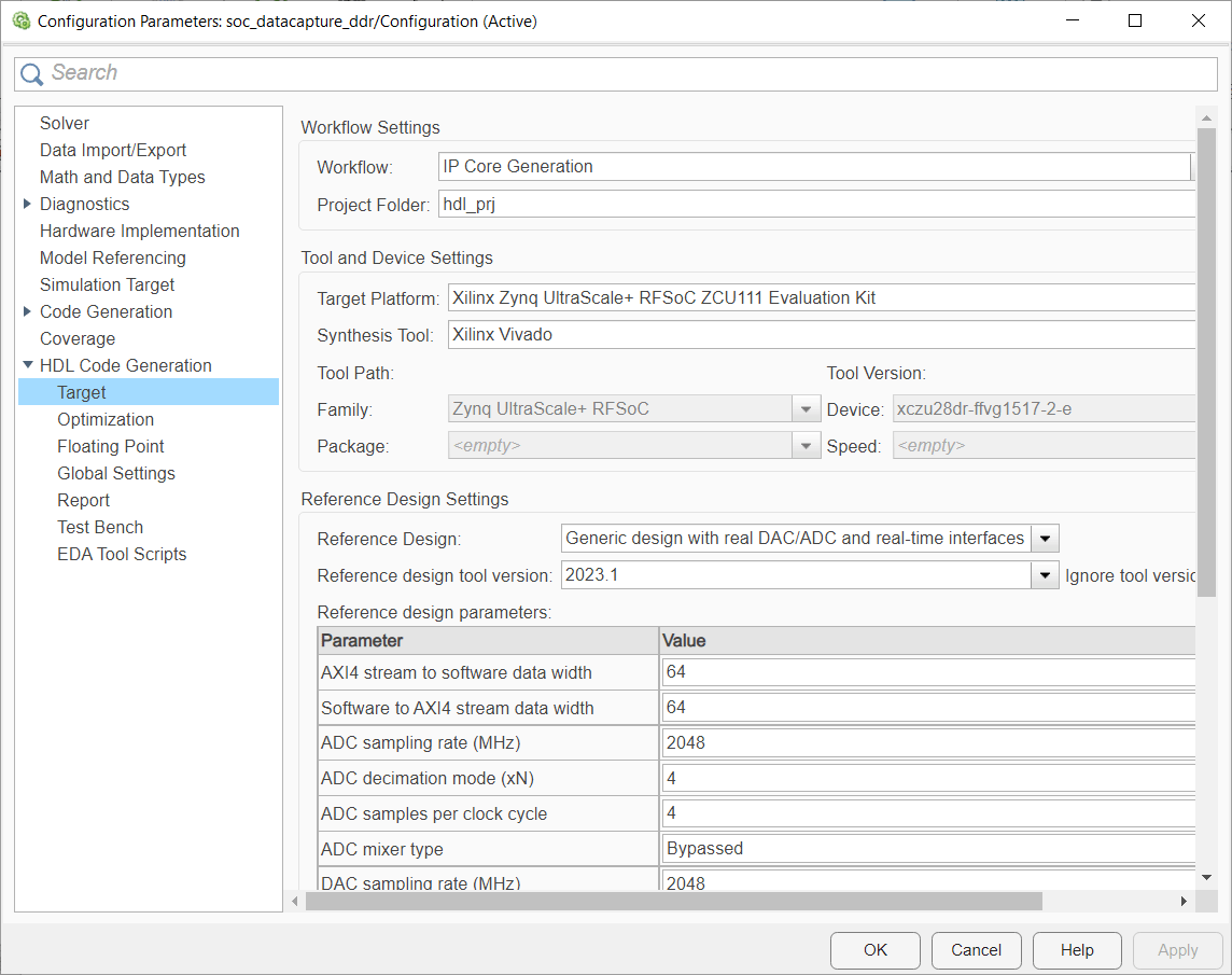
In the Configuration Parameters dialog box of the model, set the HDL workflow, target platform, and reference design by following these steps.
1. In the left pane, expand HDL Code Generation and then select Target.
2. Set Workflow to IP Core Generation.
3. Set Target Platform to Xilinx Zynq UltraScale+ RFSoC ZCU111 Evaluation Kit. Ensure that the Synthesis Tool is set to Xilinx Vivado.
4. Ensure that the Reference Design parameter is set to Real ADC/DAC Interface.
5. Ensure that the AXI4-Stream Master data width parameter under Reference Design Settings is set to 64.
6. As the model has RF Data Converter block, all the parameter values provided in RF Data Converter block are considered for code generation. If model has no block, then reference design parameters are considered for code generation.
To automatically map the interface of the IP, follow these steps.
1. Identify the IP core subsystem for code generation by selecting the Transmit and Receive Tone subsystem.
2. On the System on Chip tab, click Map Interfaces.

To view and edit the generated IP core interface mapping, follow these steps.
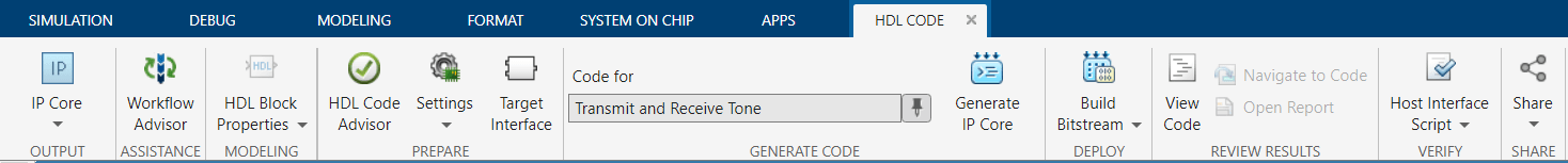
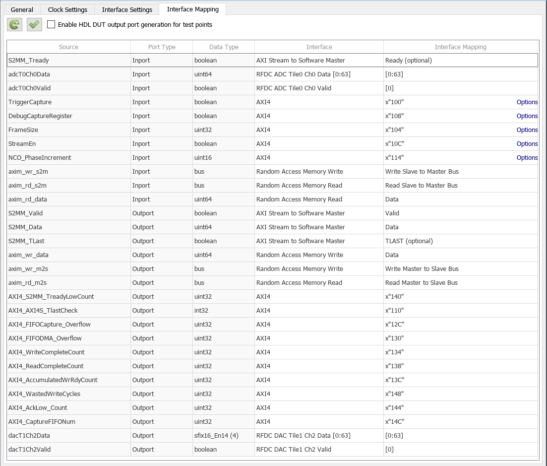
1. On the HDL Code toolstrip tab, click Target Interface.
2. In the IP Core panel, on the Interface Mapping tab, click the refresh button to load the mapping.
3. Edit the mapping until you map each DUT port and the mapping table appears as shown below.
4. Click the check button to validate the mapping.
Generate the HDL IP core and the FPGA bitstream files by following these steps.
1. On the HDL Code tab, click Build Bitstream.
2. After the HDL IP core generation finishes, an external shell opens for FPGA synthesis. Wait for the synthesis to complete. The FPGA synthesis often takes more than 30 minutes to complete.
For more information about the IP core generation workflow, see Get Started with IP Core Generation from Simulink Model (HDL Coder).
Run on Hardware
Program the FPGA on the SoC board by following these steps.
1. To download the bitstream, in the Simulink Toolstrip, on the HDL Code tab, select Build Bitstream > Program Target Device.
2. Verify your generated IP core on the hardware by using the generated host interface script. This script contains MATLAB commands that connect your hardware and interact with your IP core. To generate a host interface script file, in the Simulink Toolstrip, in the HDL Code tab, select Host Interface Script > Host Interface Script.
3. After downloading the bitstream, run the soc_datacapture_ddr_hostio_interface.m script (modified version of the generated host interface script) in the example folder to get the data back to the host from the hardware.
Summary
This example shows how to design an algorithm to write and read the captured RF samples from external DDR4 memory. You simulate and deploy the design on the Xilinx Zynq UltraScale+ ZCU111 evaluation kit. You can use this example as a reference for designing your application that requires DDR4 for data capture.
See Also
RF Data Converter | AXI4 Random Access Memory