Memory and Register Data Transfers
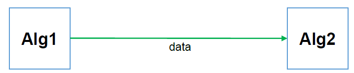
An SoC application is composed of one or more algorithms. When an algorithm transfers data to another algorithm, the data is represented as a signal line in Simulink®. For behavioral models, the data transfer is instantaneous.
This diagram shows a behavioral model of a datapath between two algorithms.
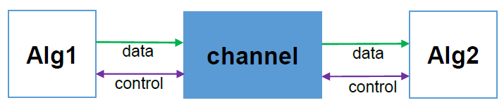
In the physical world, the algorithms can be on two separate devices, and data transfers do not happen instantaneously. Furthermore, the algorithms can run at different rates, and therefore require buffering and control logic for handshaking. For example, a simple handshake such as “data is valid” from the producer of the data and “ready to accept data” from the consumer serve as control logic.
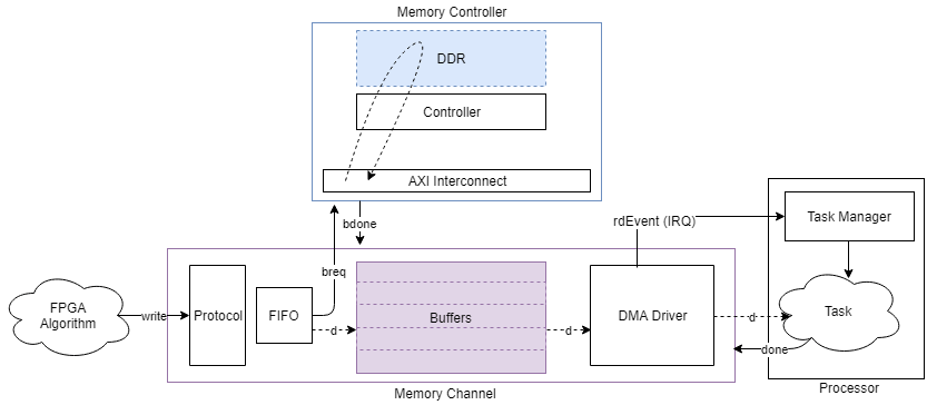
If one processing element executes in an FPGA or ASIC, and the next processing element executes on an embedded processor, then a simple signal line represents more than just a complex hardware datapath. The data transfer also represents a processor interrupt handler, an operating system task scheduler, and a software driver stack.
In SoC Blockset™, you model data transfers and handshake protocols through shared memory. Use one of these blocks for simulation of external memory:
Use a Register Channel block for register transfers.
Modeling Datapath with Memory Blocks
The memory blocks represent an abstraction to a complex datapath through external memory and support different handshake protocols. The blocks facilitate a refinement of the communication between processing elements from an instantaneous, protocol-less wire to a full direct memory access (DMA) connection between a processor and an FPGA.
By adding a memory block, you can model data movement from one part of the algorithm to another.
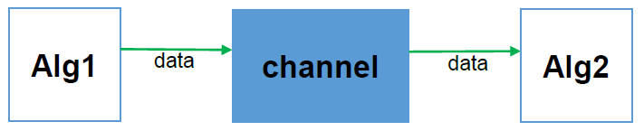
The blocks provide a model of the communication pipeline. They also provide a signaling interface.
The interface protocol depends on where the processing is executed. An FPGA or ASIC algorithm can perform data transfers by using standard protocols such as AXI4-Stream or AXI4. An embedded CPU algorithm can use a driver-interface exported to the user space.
This figure shows a model of the datapath from an FPGA algorithm streaming data to a processor algorithm.
Various memory blocks model common datapaths through external memory.
AXI4 Random Access Memory — Models random access reads and writes to external memory.
AXI4-Stream to Software — Models a stream from FPGA to a processor via external memory.
Software to AXI4-Stream — Models a stream from the processor to an FPGA via external memory.
AXI4 Video Frame Buffer — Models a video stream of full frames between two hardware algorithms via external memory.
Modeling Datapath with Register Channel Block
The Register Channel block represents the serialization of the processor reads or writes through a common configuration bus such as AXI-Lite.
The Register Channel block provides a timing model for the transfer of register values between processor and hardware algorithms through a common configuration bus. Use this block when the processor writes a command or configuration register or when the processor reads a status register.
See Also
AXI4 Random Access Memory | AXI4-Stream to Software | Software to AXI4-Stream | AXI4 Video Frame Buffer | Register Channel