Design and Implementation of Frequency Scanning Array
This example shows you how to design and implement a four-element frequency scanning array, which is used for scanning the beam by altering the frequency. The phase shifts needed at the antenna ports are dependent on frequency, and the number of phase shifters is determined by the size of the array. This technique employs transmission lines as phase shifters to incrementally adjust the phase between each antenna port relative to the frequency.
The model allows for the exploration and optimization of different antenna configurations to achieve desired results. Two approaches are discussed in this example. The first approach uses the Ideal elements from the RF Blockset™ Circuit Envelope library and the second approach uses the RF PCB Block to model the components using the catalog elements from RF PCB Toolbox™.
Antenna Array Configuration
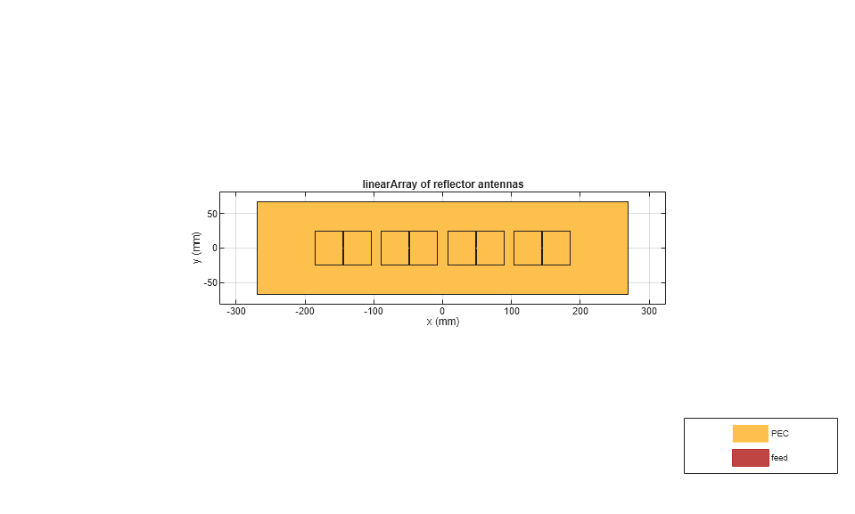
First step in designing the frequency scanning array is to design the antenna array elements. This example uses the linear array of blade dipole antenna. To do this, use the dipoleBlade object to create a linear array which is backed by an reflector object. Use the show function to visualize the array.
freq = 2e9;
d = dipoleBlade(Tilt=90, TiltAxis='Y');
ant = design(reflector(Exciter=d),freq);
antarray = design(linearArray(NumElements=4),freq,ant);
figure
show(antarray);
view([0 90])
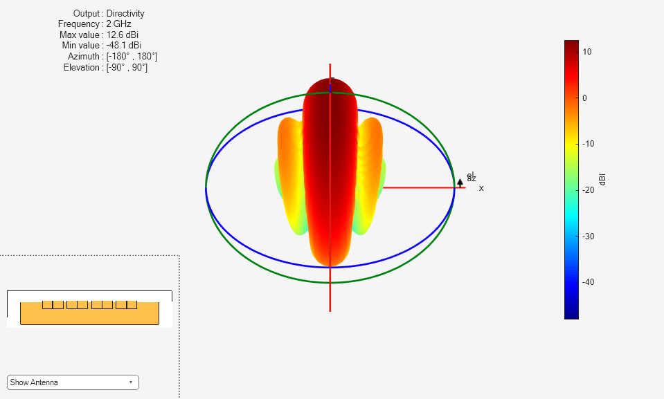
Use the pattern function to plot the radiation pattern.
figure
pattern(antarray,freq);
view([180 140]);
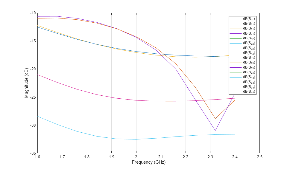
Use the sparameters function to calculate the S-parameters for the array and visualize the S-parameters using the rfplot function.
sparam = sparameters(antarray,linspace(1.6e9,2.4e9,11));
figure
rfplot(sparam);
% The s-parameters of the antenna are used in the system level simulation.
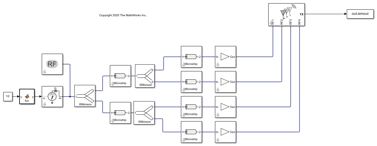
Beam-Scanning with Ideal Distributed Components
The first approach uses Ideal elements to build the frequency scanning model which has a four-element linear array of reflector-backed blade dipoles. This model uses the power dividers and the microstrip lines to create incremental phase shifts between the antenna ports, enabling beam scanning as the frequency varies from 1.6 GHz to 2.4 GHz.
Notice that at 2 GHz, there is no phase shift, leading to a boresight radiation pattern. As the frequency changes, the beam shifts, achieving a total scan angle of approximately 60 degrees over an 800 MHz bandwidth. This approach allows for efficient simulation and optimization of the antenna design. The transmissions lines are modeled with an analytical model.
Open the RF Blockset Model with the Ideal Elements.
open_system('FreqScanningIdeal.slx');
The code below calculates the pattern at different frequencies by looping through each value of the angle and calculating the transmitted power at every value. The data that is generated by this code is saved in a MAT file and used in this example.
freq1 = 1.6:0.2:2.4;
for i = 1:numel(freq1)
   freq = freq1(i)*1e9;
   p = pattern(antarray,freq);
   for j=1:numel(theta1)
       theta = theta1(j);
       out = sim('FreqScanningIdeal.slx',0);
       data1(i,j) = abs(out.simout.Data(:,:,1));
       data2(i,j) = abs(out.simout.Data(:,:,2));
   end
end
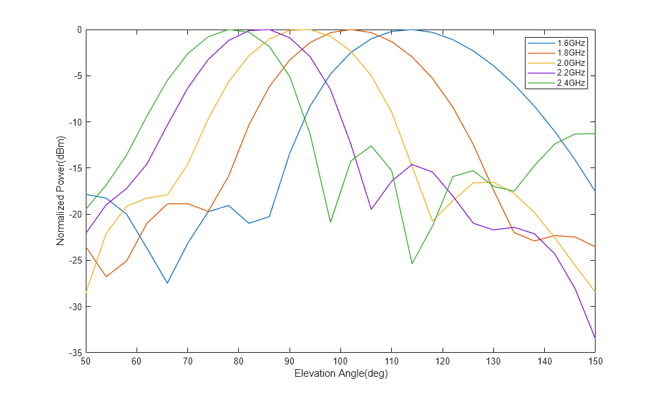
Load the MAT file and plot the data to visualize the beam scanning behavior. Use the plot function to plot the Angle vs. Normalized power transmitted. The plot shows that the Array beam is scanned from 70 deg to 110 deg when the frequency is changed from 1.6 GHz to 2.4 GHz. The data1 and data2 variables contain the data for the Radiated power in both the orthogonal polarizations.
 load('Ideal.mat')
theta1 = 50:4:150;
a = data1+data2;
a = 20*log10(a);
a1 = a(1,:)-max(a(1,:));
a2 = a(2,:)-max(a(2,:));
a3 = a(3,:)-max(a(3,:));
a4 = a(4,:)-max(a(4,:));
a5 = a(5,:)-max(a(5,:));
figure,plot(theta1,a1,'LineWidth',1);
hold on
plot(theta1,a2,'LineWidth',1);
plot(theta1,a3,'LineWidth',1);
plot(theta1,a4,'LineWidth',1);
plot(theta1,a5,'LineWidth',1);
legend('1.6GHz','1.8GHz','2.0GHz','2.2GHz','2.4GHz');
xlabel('Elevation Angle(deg)');
ylabel('Normalized Power(dBm)');
Frequency Scanning Using RF PCB Components
The second approach to design a frequency scanning array is to use the RF PCB Block from the Circuit Envelope Library. RF PCB block enables to use components that are solved using a full wave MoM solver. The Ideal Components like microstrip line and wilkinson power dividers can be replaced with an equivalent RF PCB objects.
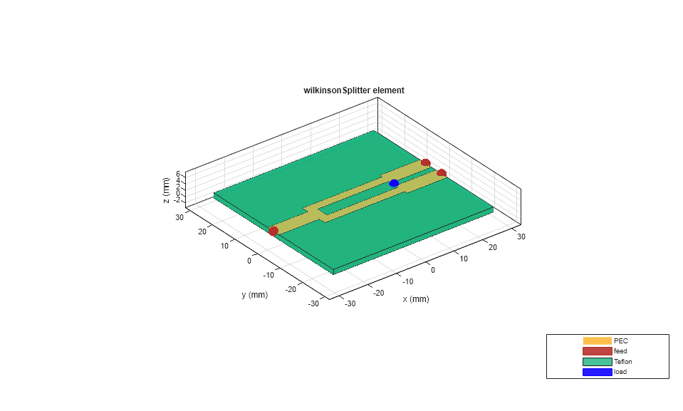
Use the microstripLine and the wilkinsonSplitter objects and design them at the required frequency. Create the wilkinsonSplitter and visualize it using the show function.
freq = 2e9;
wilk = design(wilkinsonSplitter,freq);
figure
show(wilk);
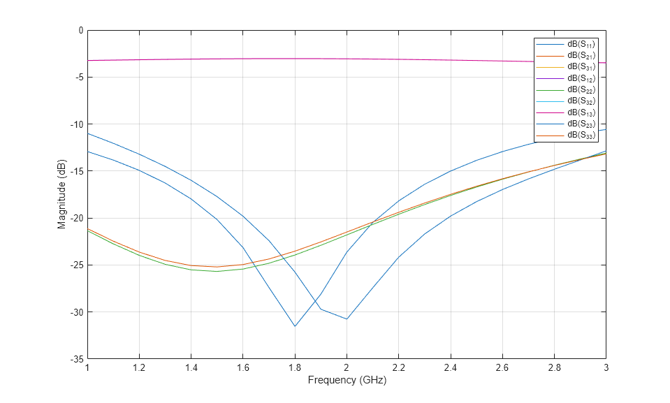
Use the sparameters function to calculate the S-parameters using the MoM solver and plot them using the rfplot function.
spar = sparameters(wilk,linspace(1e9,3e9,21));
figure
rfplot(spar);
Use the design function to design the microstrip lines with different line lengths in terms of wavelength.
sub = dielectric('Teflon');
sub.EpsilonR = 2.2;
h = 0.635e-3;
mline1 = design(microstripLine(Substrate=sub,Height=h),freq,LineLength = 1);
mline2 = design(microstripLine(Substrate=sub,Height=h),freq,LineLength = 2);
mline3 = design(microstripLine(Substrate=sub,Height=h),freq,LineLength = 3);

Use the sparameters function to calculate the S-parameters of the three microstrip lines.
spar1 = sparameters(mline1,linspace(1e9,3e9,21));
spar2 = sparameters(mline2,linspace(1e9,3e9,21));
spar3 = sparameters(mline3,linspace(1e9,3e9,21));
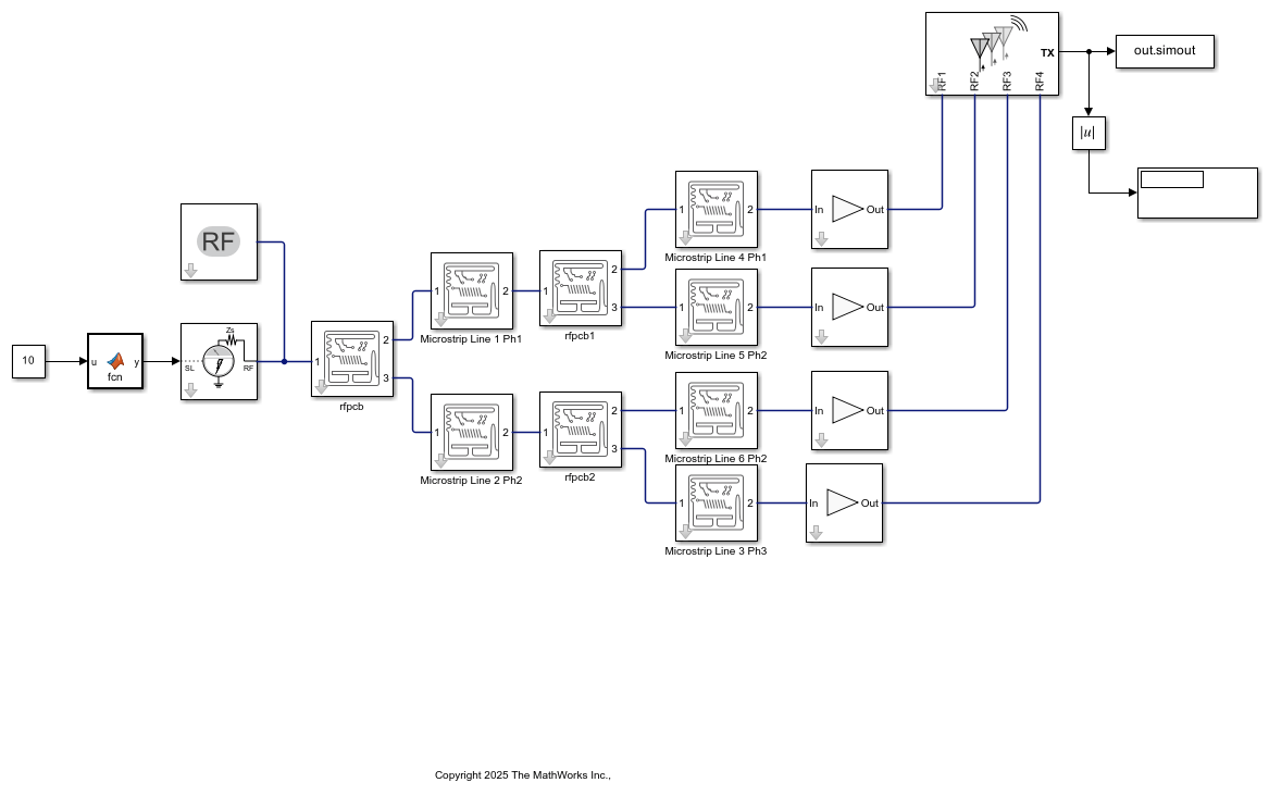
Replace the RF transmission line blocks with the RF PCB blocks. Use the mline1, mline2, and mline3 as input to the three RF PCB blocks.
Open the RF Blockset Model with the RF PCB Block.
open_system('FreqScanningRFPCB');

The below code calculates the pattern at different frequencies by looping through each value of the angle and calculating the transmitted power at every value. The data that is generated by this code is saved in a MAT file.
freq1 = 1.6:0.2:2.4;
for i = 1:numel(freq1)
freq = freq1(i)*1e9;
p = pattern(antarray,freq);
for j=1:numel(theta1)
theta = theta1(j);
out = sim('FreqScanningRFPCB.slx',0);
data1(i,j) = abs(out.simout.Data(:,:,1));
data2(i,j) = abs(out.simout.Data(:,:,2));
end
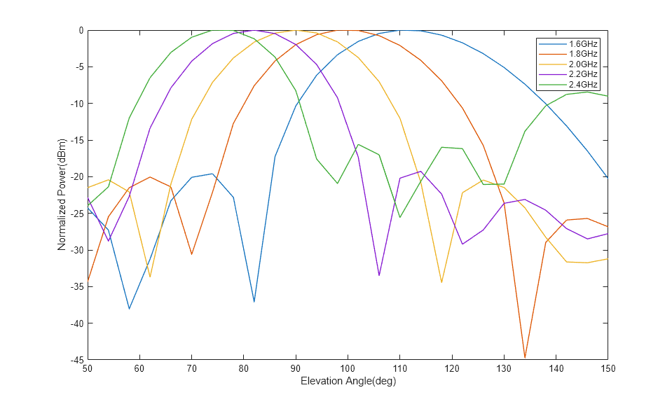
endLoad the MAT file and plot the data to visualize the beam scanning behavior. Use the plot function to plot the Angle vs. Normalized power transmitted. The plot shows that the Array beam is scanned from 70 deg to 110 deg when the frequency is changed from 1.6 GHz to 2.4 GHz.The data1 and data2 variables contain the data for the Radiated power in both the orthogonal polarizations.
load('rfpcb.mat');
theta1 = 50:4:150;
a = data1+data2;
a = 20*log10(a);
a1 = a(1,:)-max(a(1,:));
a2 = a(2,:)-max(a(2,:));
a3 = a(3,:)-max(a(3,:));
a4 = a(4,:)-max(a(4,:));
a5 = a(5,:)-max(a(5,:));
figure,plot(theta1,a1,'LineWidth',1);
hold on
plot(theta1,a2,'LineWidth',1);
plot(theta1,a3,'LineWidth',1);
plot(theta1,a4,'LineWidth',1);
plot(theta1,a5,'LineWidth',1);
legend('1.6GHz','1.8GHz','2.0GHz','2.2GHz','2.4GHz');
xlabel('Elevation Angle(deg)');
ylabel('Normalized Power(dBm)');

Conclusion
This example shows the frequency scanning array using both ideal RF elements and RF PCB elements. With ideal RF elements, maximum radiation occurs precisely at 90 degrees, whereas with the RF PCB elements, the maximum radiation is shifted. Using this two-design approach, you can use the various types of dividers and transmission lines from RF PCB Toolbox to validate the design, enabling comprehensive system simulations in RF Blockset.
References
[1] S. Joshi, S. Kulkarni and V. Iyer. "Model Based Design for Frequency Scanning Array". 2023 IEEE/MTT-S International Microwave Symposium - IMS 2023, San Diego, CA, USA, 2023, pp. 819-822, doi: 10.1109/IMS37964.2023.10187977.