LLC Resonant Converter Operating Point Analysis
This example shows how to perform the operating point analysis of an LLC resonant converter power supply using the Mixed-Signal Blockset™.
Sections
Introduction - States the overall subject of this example.
LLC Resonant Converter - Introduces the full bridge LLC resonant converter circuit used in this example.
Time Domain Model - Introduces the construction of the time domain model used to explore the circuit's waveforms and validate the operating point results.
Modes of Operation - Introduces the waveforms associated with the Boost, Resonant, and Buck modes of operation for the LLC converter.
Operating Point Analysis - Performs the operating point analysis, first for a single set of operating conditions and then for a multi-dimensional space of operating conditions.
Operating Point Validation - Compares the DC output of the circuit as predicted by operating point analysis to the output observed from time domain simulations.
Switching Losses - Discusses some of the details of the switching waveforms and their effect on switching losses.
Introduction
LLC resonant converters are widely used because they can minimize switching losses and therefore operate at higher efficiencies than power supplies with other circuit topologies. However the analysis of these circuits is made much more difficult by the fact that the resonant frequency of the circuit is designed to be in the same frequency range as the circuit's control signals, invalidating the state space averaging methods [1, chapter 7] applied to most other power supplies.
Another widely used approach is first harmonic analysis [2]. This approach produces accurate results near the resonant frequency of the circuit, with diminishing accuracy as the control frequency gets further from the resonant frequency.
The operating point analysis in this example demonstrates a mathematically more complex approach [3] that is valid for an LLC resonant converter and other resonant or quasi-resonant circuit topologies.
This example is one segment in a sequence of examples that demonstrate a comprehensive power supply design workflow applicable to LLC resonant converters. The circuit used in this example follows closely the circuit topology and element values used in the Simscape LLC design example. The Control System Toolbox controller design example demonstrates how to use data and small signal models from operating point analyses such as the ones in this example to design a single power supply controller to operate over a wide range of input voltages, output voltages, load resistances and load currents.
LLC Resonant Converter
The LLC resonance converter circuit topology used in this example is the full bridge topology shown in the Simscape diagram below.
schematic = 'LLC_FullBridge_MSB';
load_system(schematic);
open_system(schematic);
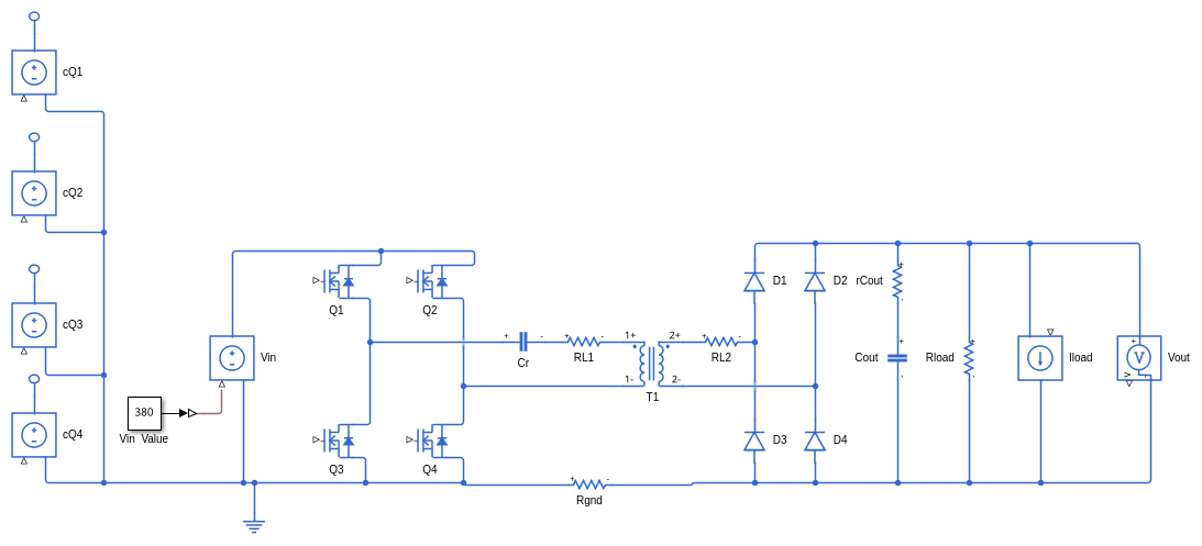
The circuit is the concatenation of three subcircuits: a full bridge inverter formed by MOSFETs Q1, Q2, Q3, and Q4, a resonant tank formed by Cr and T1, and a full bridge rectifier formed by diodes D1, D2, D3, and D4 combined with decoupling capacitor Cout.
The inverter transforms the DC input Vin into a square wave applied to the resonant tank. The resonant tank filters the square wave and applies it through an isolating transformer to the rectifier. The rectifier transforms the resonant tank wave back into a DC voltage that is then applied to the load.% The control input to the inverter is an idealized behavioral model of the gate drive, where the voltage sources cQ1, cQ2, cQ3 and cQ4 determine whether the gate drives to the corresponding transistors have turned the transistor on or off.
The resonant frequency of the resonator tank is determined by the series resonance of the capacitor Cr with the leakage inductance of the transformer T1. For the circuit design in this example the tank resonant frequency is 100kHz.
The amplitude of the wave at the output of the resonant tank is a function of the control frequency, the frequency response of the resonant tank, and the turns ratio of the transformer. The DC output is controlled by varying the control frequency.
Consistent with the Simscape LLC design example, three different values for the load resistance Rload are analyzed in this example: 30.625, 20.417 and 12.25 ohms. The additional load current Iload is zero in all cases and is included in the model to evaluate the small signal output impedance of the power train. The model delivered with this example has the load resistance set at 12.25 ohms.
Time Domain Model
In the Mixed-Signal Blockset the LLC resonant converter is modeled as a switched linear system. The circuit has a number of switch states determined by the on/off states of the MOSFETs and diodes, and the circuit is assumed to be linear in any one of these switch states. The linear state vector has the same definition in every one of the switch states, so that switching between switch states does not cause glitches. This model is reasonably accurate, enables rigorous mathematical analysis, and runs efficiently in a time domain simulation.
You can use the LLC_FullBridge_OL Simulink model to run the LLC_FullBridge_MSB circuit open loop in a time domain simulation. Use the following script to open the model and then create or reconstruct a block that models the LLC resonant converter in the Simulink model.
model = 'LLC_FullBridge_OL';
load_system(model);
open_system(model);

circuit = cktconfig(schematic);
blockpath = cktblock(circuit,model, ...
    Ports = {'cQ1','cQ2','cQ3','cQ4','Vin','Iload','Vout'},...
    CircuitDesignName ='Full Bridge LLC',...
    BlockName ='Power Train');

connectllc;

set_param(blockpath,'InheritSampleRate','off');
set_param(blockpath,'SampleRate','2e7');

set_param(blockpath,'DebugMode','on');
set_param(blockpath,'DebugStart','0.02897');
set_param(blockpath,'DebugStop','0.029');
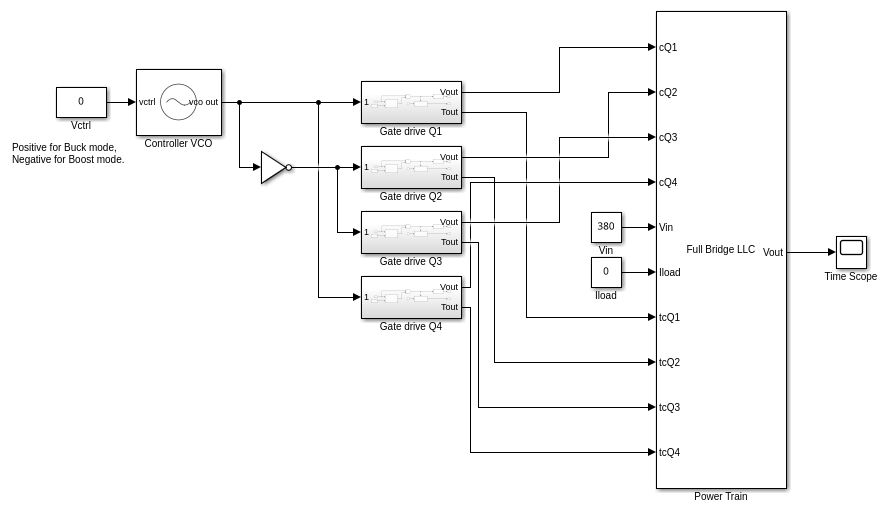
In most practical applications you will connect the block to the rest of the block manually; however in this example the connectllc script does that for you.
In this Simulink model it is the LLC resonant converter block that defines the sample rate for the simulation, and so the 'InheritSampleRate" and 'SampleRate" parameters must be set.
Also, the Mixed-Signal Blockset switched circuit block offers a debug mode that will give access to every voltage or current waveform in the circuit over a time interval that you've defined. These waveforms will be used to explain the different modes of operation for an LLC resonant converter. The parameters 'DebugMode', 'DebugStart', and 'DebugStop' set up the debug mode.
To understand where each debug waveform was recorded in the circuit, construct a table that maps the names of the circuit elements to the names of the circuit nodes.
circuittbl = ckttbl(circuit);
You will find it convenient to double-click on the resulting circuit map table in the base workspace, thus displaying it in the MATLAB variable display window.
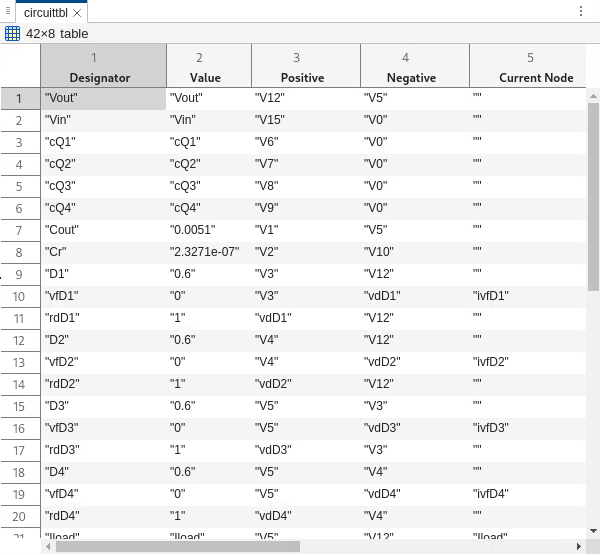
Note that this table includes data for the equivalent circuits used internal to the circuit solution. This includes the individual transformer windings T1L1 and T1L2 as well as the equivalent series resistance and diode voltage drop for the MOSFETs and diodes. For example the diode D1 is modeled as the resistor rdD1 in series with the diode forward voltage drop vfD1. Note also that there are current nodes as well as voltage nodes. The current in the transformer winding T1L1 is recorded in the current node iT1L1. Similarly, the current in the diode D1 is ivfD1. In addition to the LLC resonant converter block, the LLC_FullBridge_OL model contains a VCO block to set the control frequency. The free running frequency of the VCO is set to 100kHz, the resonant frequency of the LLC resonant converter. The voltage sensitivity is also set to 100kHz so that the constant control voltage input to the VCO is scaled to the resonant frequency. The duty cycle of the VCO output is 0.5.
The LLC_FullBridge_OL model also contains a separate gate drive subcircuit for each MOSFET in the circuit. Double click on one of these gate drive subcircuits to see the gate drive design.
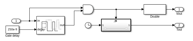
The gate drive subcircuit applies a delay to the rising edges of the input using a delay line/AND gate configuration that is very similar to the way gate delays are implemented in production circuitry. This gate delay is used to create a "dead time" between the time one transistor turns off and another transistor turns on. The gate delay in this case is 250ns. It is important to choose a gate delay that will prevent two transistors in series from being on at the same time.
The gate drive subcircuit also contains a triggered subsystem that detects the exact times that the gate drive transitions occur. This time is input to the LLC resonant converter block along with the gate drive signal so that the block can make precise switch state transitions between sample times. The block calculates from the current sample time to the precise transition time, transitions to a different switch state, and then calculates to the next sample time.
Modes of Operation
The operating point analysis will be performed for a range of control frequencies. The control frequency range for this example was chosen to evaluate the output in all three primary modes of LLC resonant converter operation: Boost, Resonant and Buck. This section shows you how to use the debug output from the time domain model to view the detailed internal circuit waveforms for these modes.
To view the waveforms for the Resonant mode, set the control voltage to zero, thus producing a 100kHz frequency from the VCO. Then run the model.
set_param([model '/Vctrl'],'Value','0');
sim(model);
open_system([model,'/Time Scope']);
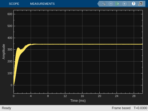
Given the nominal input voltage of 380 volts and a control frequency equal to the resonant frequency of the tank, the power train produces approximately the nominal output voltage of 350 volts.
In addition to the output voltage display, the Power Train block has constructed a Waves struct and a Header struct in the base workspace. Use these structs to construct a timeseries object containing the debug waveforms, then launch the Simulink Data Inspector.
tbl = array2table(Waves,"VariableNames",Header);
debugout = table2timetable(tbl,"RowTimes",seconds(tbl.Time));
Simulink.sdi.view;
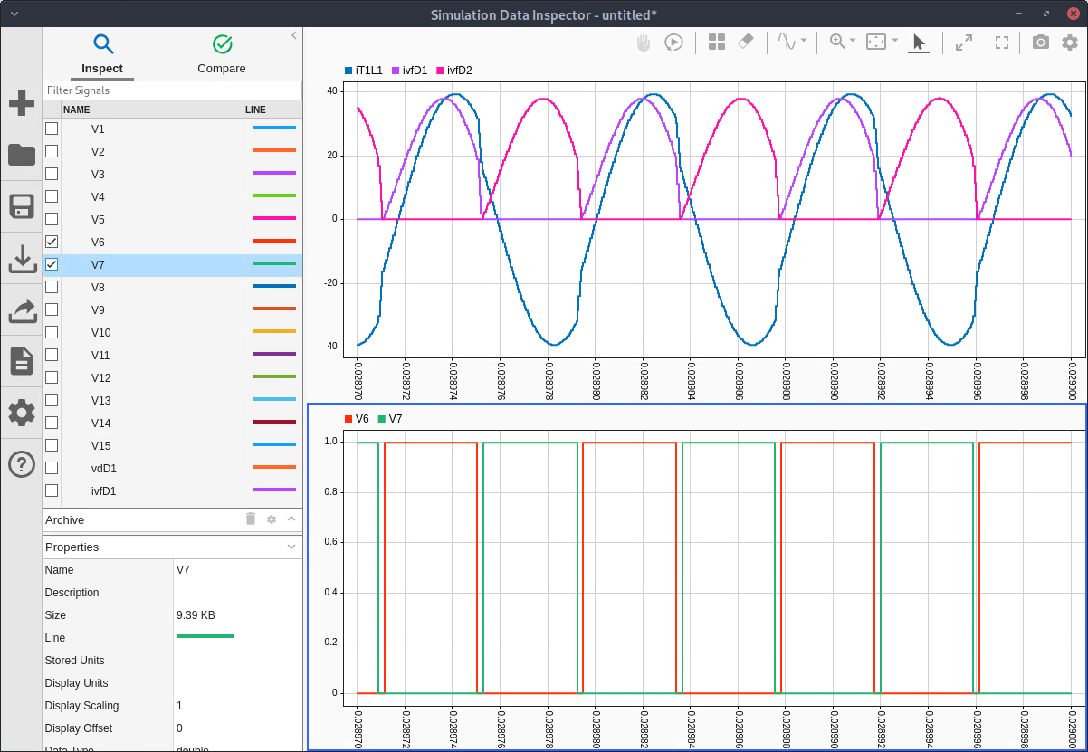
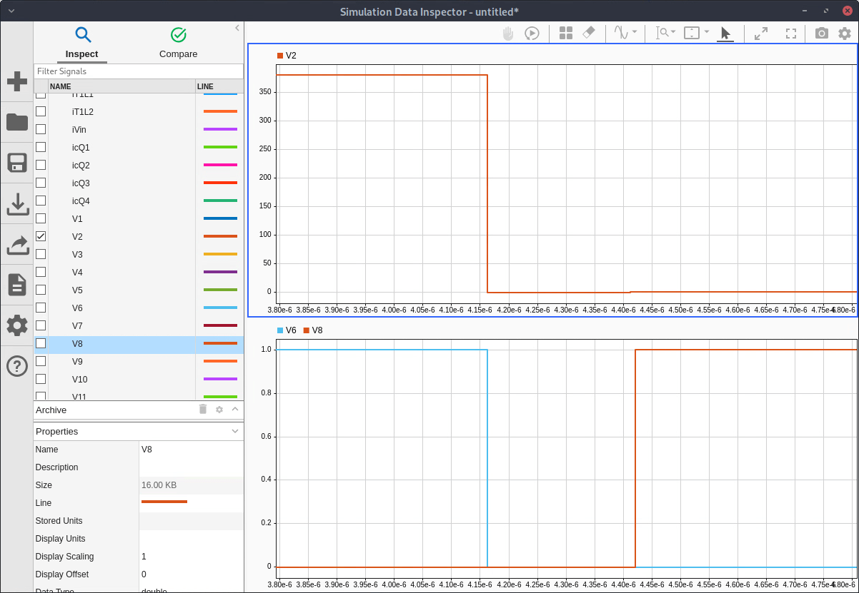
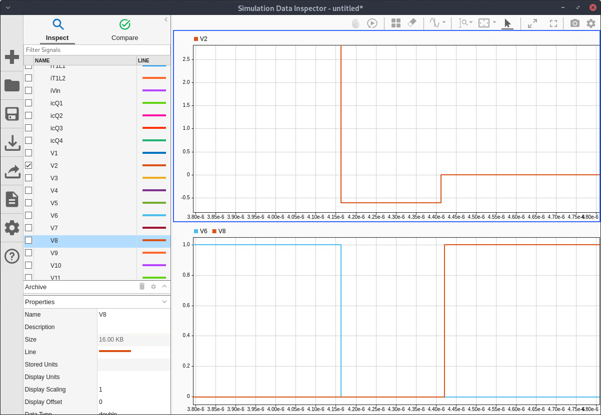
In the Simulink Data Inspector, choose the iT1L1, ivfD1 and ivfD2 current waveforms for the upper window and the control waveforms V6 (for cQ1) and V7 (for cQ2) for the lower window.
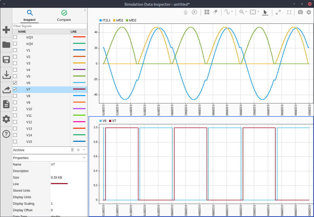
Note that in Resonant mode the transformer current is very nearly sinusoidal, and the diode currents approximate those of a rectified sine wave. The diode currents at the end of each half cycle reach zero. This behavior is called zero current switching (ZCS), and the diode switching losses under these conditions are negligible.
You can repeat this process for Boost mode by setting the VCO control voltage 'LLC_FullBridge_OL/Vctrl' to '-0.2', thus producing a control frequency of 80 kHz.
set_param([model '/Vctrl'],'Value','-0.2');
sim(model);
open_system([model,'/Time Scope']);
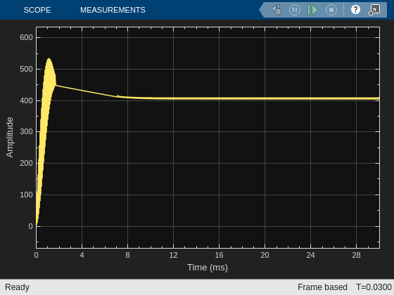
Under these conditions the output voltage is a little more than 400 volts, demonstrating why this mode is called the Boost mode.
The corresponding waveforms are
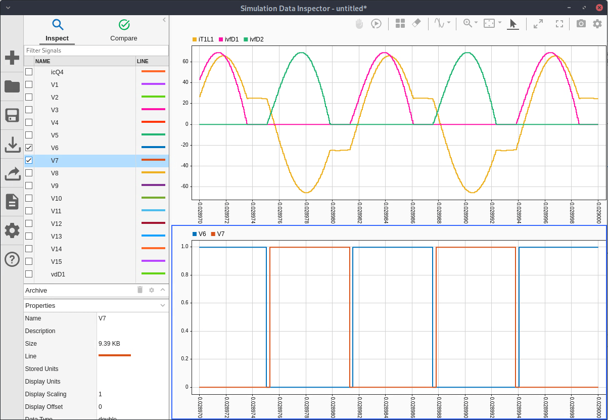
For this mode the transformer current becomes nearly constant at the end of each resonant half cycle, and the diode currents follow the same shape, with zero diode current in either diode between diode current pulses. This is also ZCS.
Similarly, you can repeat this process for Buck mode by setting 'LLC_FullBridge_OL/Vctrl' to '0.2', thus producing a control frequency of 120 kHz.
set_param([model '/Vctrl'],'Value','0.2');
sim(model);
open_system([model,'/Time Scope']);
Under these conditions the output voltage is a little more than 300 volts, demonstrating why this mode is called Buck mode.
For this mode the transformer current does not complete its half cycle before the end of one half of the switching cycle and makes a rapid transition to begin the next half cycle. While the diode current does reach zero at the end of each half cycle, the rapid rate at which it reaches zero leaves the value of the switching losses in doubt. Experts disagree as to whether this behavior can be called ZCS. The Switching Losses section of this example offers some insight into the diode switching in Buck mode but does not propose any definitive conclusions.
Operating Point Analysis
You can very efficiently obtain the circuit's operating point using the cktoperpoint function. It's useful to start by clearly defining the operating point conditions.
vin  = 380;
vout = [380,350,320];
rload = 12.25;
iload = 0;
Next, construct a circuit object that contains the name/value pairs that define the basic operating point setup. If there are circuit element values such as Rload that must be defined for the operating point analysis and may vary between operating point analyses, set the parameters for those element values before constructing the circuit object.
open(schematic);
set_param([schematic '/Rload'], 'R', num2str(rload));
circuit = cktconfig(schematic, ...
    Ports = {'cQ1','cQ2','cQ3','cQ4','Vin','Iload','Vout'},...
    CircuitDesignName = 'Full Bridge LLC',...
    BlockName = 'Power Train',...
    OutputPort = 'Vout',...
    ControlVariable = "Frequency", ...
    DutyCycle = 0.5, ...
    PhaseOffsets = '[0, 0.5, 0.5, 0]', ...
    PulseDuration = '[0.5-0.25e-6*f, 0.5-0.25e-6*f, 0.5-0.25e-6*f, 0.5-0.25e-6*f]', ...
    WaveSamples = 1024 );
Perform the operating point analysis for this specific set of conditions. The specified output values are intended to operate in boost, resonant, and buck modes, respectively. Note that although in this example the value for the OutputValues name/value pair is an array of desired output values, it often is a scalar.
[dcresults,plotdata,waves,ssmodels,abcd] = cktoperpoint(circuit, ...
    OutputValues = vout, ...
    Frequency = [0.7e5 1.3e5], ...
    InputValues = {"Vin","Iload";vin,iload});
The outputs from this analysis are
dcresults - A table containing the inputs and outputs for each element of the OutputValues name/value pair in the operating point analysis.
plotdata - A two column matrix containing the data plotted in the operating point plot.
waves - A cell array of tables, one for each element of the OutputValues name/value pair. Each table contains a one switching cycle steady state waveform for every voltage and current in the circuit.
ssmodels - A Control System Toolbox ss small signal linear model if only one output value was specified, or a cell array of ss models, one for each element in the OutputValues name/value pair, if an array of output values was specified.
abcd - A struct array containing the data used to construct the ss models.
These outputs enable a wide range of detailed steady state circuit analyses such as efficiency, ripple, or power dissipation for each circuit element. See the Boost power train example for more details.
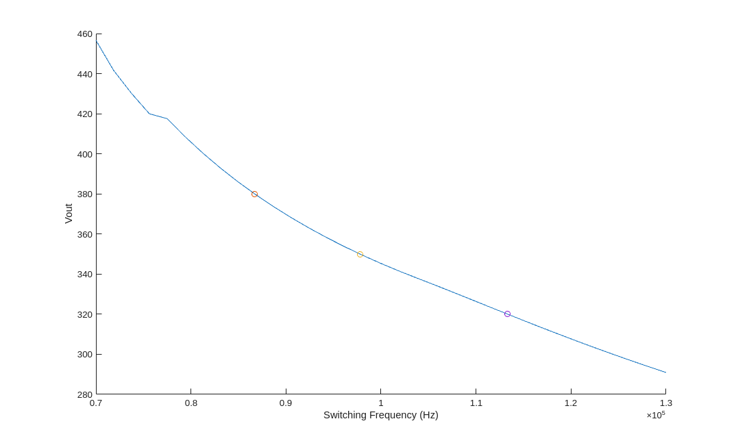
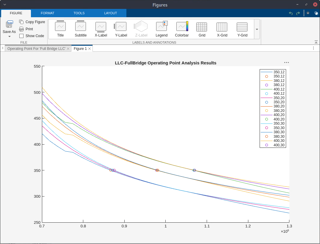
You can also run scripts to perform operating point analysis for a circuit under a wide range of conditions such as those contained in a performance specification or those needed to design a robust power supply controller. The script opstudy.m included with this example is one such script. It evaluates the operating point for each combination of three different values of load resistance (12.25 ohms, 20.417 ohms, 30.625 ohms) and three different input voltages (350V, 380V, 400V). The results are contained in the file LLC_OP_study.mat included with this example and are shown in the plot below.
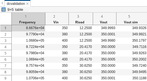
DC Validation
You can validate the operating point analysis results by comparing them to values obtained through time domain simulation. From the circuit table presented earlier in this example you can see that the output voltage Vout is between voltage nodes V12 and V5. The waveforms for these nodes are included in the debug waveforms produced by the time domain simulation and can be averaged to obtain a precise DC output voltage.
The script opvalidate.m, included with this example, performs these actions and adds a "Vout sim" column containing the time domain simulation results to the dcresults table, producing a dcvalidation table.
Switching Losses
The circuit model used in this example does not include the details that cause switching losses. However you can gain some insight into the behavior of the switching losses in this circuit by reviewing the waveforms applied to the switching loss mechanisms.
For this analysis we will use the single switch cycle waveforms produced by the operating point analysis because they use a smaller sample time. Since we will study buck mode switching losses, we will use the waveforms from the buck mode operating point.
opwaves = waves{3};
optable = table2timetable(opwaves,"RowTimes",seconds(opwaves.Time));
Simulink.sdi.view;
The primary switching loss mechanism in MOSFETs is the discharging of the drain-source parasitic capacitance by the transistor. When this happens the resistive impedance of the transistor's channel causes the energy stored in the parasitic capacitance to be dissipated as heat in the transistor. The switching loss is a quadratic function of the voltage at the time the transistor turns on, and the ideal condition is to have the drain-source voltage at zero at the time the transistor turns on, a condition referred to as zero voltage switching (ZVS).
The switching conditions for Q3 are typical of the conditions for all the transistors. Q3 is turned on a gate drive dead time after Q1 has been turned off. From the circuit map table you will see that Q3 is connected between V2 and V0 (the reference node), the cQ3 gate drive is at V8, and the cQ1 gate drive is at V6. You can therefore display in the Simulink Data Inspector the sequence of events that lead up to the Q3 turn-on.
When Q1 is turned off (through V6) the transformer inductance T1L1 drives V2 to decrease until the body diode of Q3 turns on. V8 turns Q3 on after that. You can expand the vertical scale to see the details of the body diode waveform as it decreases below the source voltage V0. Q3 turns on in close to ZVS conditions and most of the energy in the parasitic capacitance has been pumped back into V0 (reference voltage).
Note that in the detailed circuit design it is important to incorporate the total parasitic capacitance, the supply voltage Vin and the body diode forward conductivity into the calculation of a gate drive dead time that will ensure ZVS conditions.
The inductor current will cause ZVS for the pull-up transistor in most SMPS power trains. However ZVS will only occur in the pull-down transistor if the inductor current changes sign before the pull-down transistor is turned on. The resonant behavior of the LLC converter creates this condition, causing ZVS for all of the transistors in the inverter subcircuit.
Diode switching losses are caused by the stored charge and recovery time of the diode. During turn-off, the diode continues to conduct until the minority carriers in its junction have been recombined. Part of this period occurs after the diode has become reverse biased but the diode conductivity continues to be significant.
In Buck mode (e.g., control frequency equals 113 kHz), the diode currents have not reached zero by the time the transistors have been turned off on the primary side of the transformer. A complex sequence of events then ensues. You can follow this sequence of events in a waveform display containing the gate drive signals (V6 and V8), the transformer primary voltages (V10 and V14), the transformer primary current (iT1L1), the transformer secondary current (iT1L2), and the transformer secondary voltage (V3 and V4).
1. The gate control voltages turn off all transistors.
2. The transformer primary voltage shifts from positive to negative while the secondary voltage remains unchanged.
3. The primary current starts decreasing and the secondary current starts decreasing much more rapidly.
4. The diode current decreases to zero. (This occurs at a time which is independent of the gate drive dead time.)
5. The secondary voltage switches.
6. The slopes of the primary and secondary transformer currents shift back to what they were.
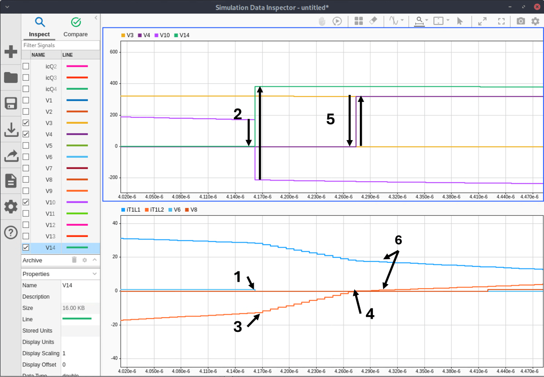
The switching losses are determined by the details of what happens in step 4 of this process. The actual diode current will lag the iT1L2 predicted by our circuit model by a time that is determined by the diode's reverse recovery time and softness factor [1, section 4.3] while the slope remains approximately equal to the value determined in step 3. So the diode current at switch time should be approximately the step 3 slope times the reverse recovery time times the softness factor.
References
[1] Erickson, Robert W., and Dragan Maksimović. Fundamentals of Power Electronics. Third edition, Chapter 7. Springer, 2020.
[2] Ivankovic, Mladen. Optimal LLC Converter Design: From First Harmonic Approximation through Design Oriented Analysis, Seminar 3, IEEE APEC 2024 conference, February 25, 2024.
[3] Chilukuri, Gopi Reddy, Dipayan Chatterjee, Ranajay Mallik, and Santanu Kapat. Discrete-Time Modeling Framework for Analysis of LLC Converters over a Wide Frequency Range. 2022 IEEE Applied Power Electronics Conference and Exposition (APEC), March 2022, 267–73. https://doi.org/10.1109/APEC43599.2022.9773487.