Real-Time Simulation of Dual Active Bridge Converter on FPGA
This example shows how to model a dual active bridge (DAB) converter with two full-bridges and control the output voltage of the circuit. The converter is modeled using the dynamic switch approximation method. You can generate HDL code for the model, synthesize the code, and deploy it onto target hardware.
Set Up Synthesis Tool Path
Before generating HDL code using HDL Coder™, set up your synthesis tool path. For example, if you use Xilinx® Vivado®, install the latest version as described in HDL Language Support and Supported Third-Party Tools and Hardware.
Then, set the tool path to the installed Xilinx Vivado executable by using the hdlsetuptoolpath function. For example, this command sets the synthesis tool path to point to your installed Vivado® Design Suite 2024.1 batch file:
hdlsetuptoolpath("ToolName","Xilinx Vivado",...
"ToolPath","C:\Xilinx\Vivado\2024.1\bin\vivado.bat")
Dual Active Bridge Converter
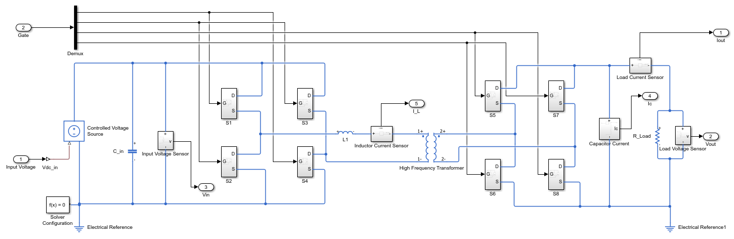
A dual active bridge (DAB) converter is a DC-DC converter that provides bidirectional power flow applications for battery systems, renewable energy, solid-state transformers, and low- to medium-voltage grid applications. A DAB converter is designed using two full-bridges that are separated by a high-frequency transformer and an inductor. Depending on the control strategy, a DC-blocking capacitor may also be included.
This example shows the topology of a DAB converter that generates a DC output voltage from a DC input voltage of 800V, thus working as a DC-DC converter. The primary switch is an ideal MOSFET dynamic switch from the Dynamic Switch library (SimscapeFPGAHIL_lib) that is triggered by a 50 kHz pulse with a duty cycle of 0.5. The winding ratio of the high-frequency transformer (N2/N1) is 0.625. For more information about the dynamic switch approximation method, see Generate HDL Code for Simscape Models by Using Dynamic Switch Approximation.
The most common approach to control a dual active bridge is through single-phase modulation. In this technique, each full-bridge receives a PWM signal with a duty cycle of 0.5, and the signals are phase shifted relative to one another. Increasing the phase difference between the signals increases the power flow through the converter.
Open the DAB converter model.
open_system("sschdlexDualActiveBridgeExample")
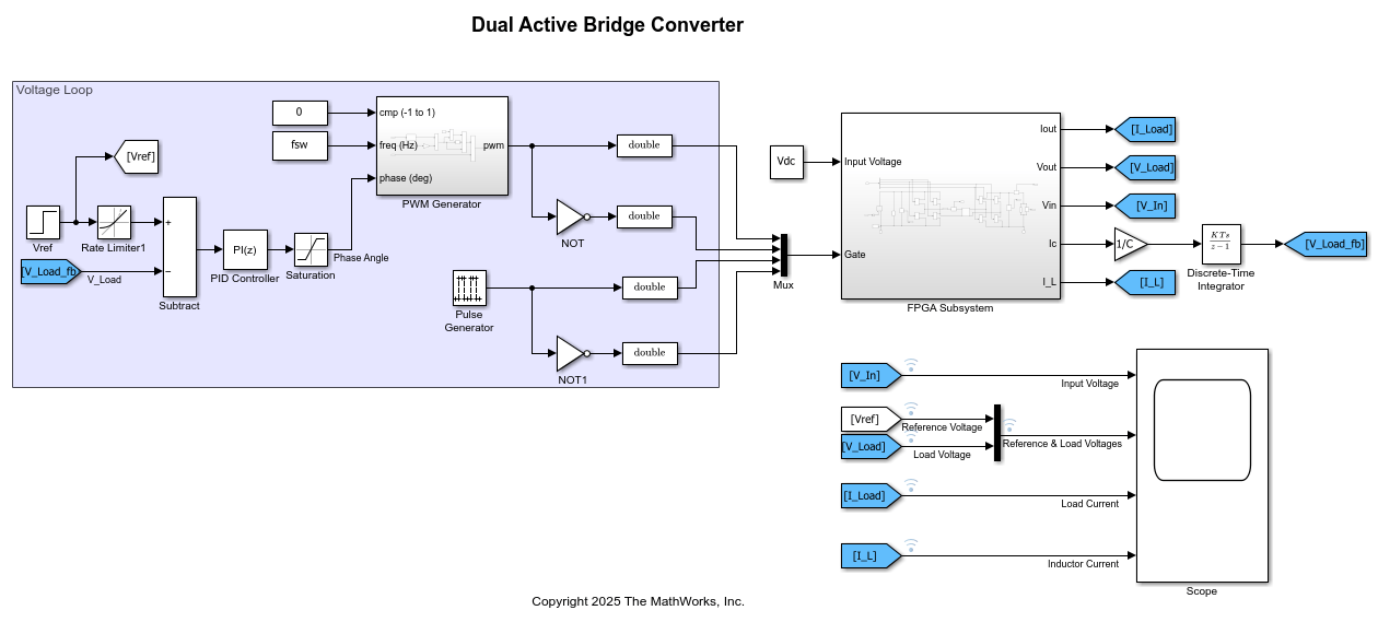
The configurations inside the FPGA Subsystem block run on an FPGA board and the components that are outside the FPGA Subsystem block run on a CPU in real time.
Open the FPGA Subsystem block that contains Simscape blocks.
open_system("sschdlexDualActiveBridgeExample/FPGA Subsystem")
Run Desktop Simulation
The input to the DAB converter model is a DC voltage  set to 800 V using the Constant block. To test different scenarios, you can change the value of this block as needed. The model is configured to run on the FPGA at a sampling frequency of 20 MHz, which corresponds to a sample time of
 5e-8 s, as specified in the Solver Configuration block.
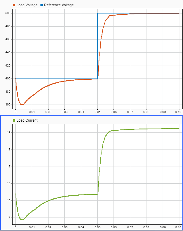
Simulate the model to view the waveforms. The Scope block displays the output voltage and inductor current waveforms. Alternatively, double-click the Data Logger on top of the output signals to open the Simulation Data Inspector.
sim("sschdlexDualActiveBridgeExample");

% Clear all plotted signals from subplots and set a 2-by-1 grid layout
Simulink.sdi.clearAllSubPlots
Simulink.sdi.setSubPlotLayout(2,1);

% Get the latest run identifiers
allIDs2 = Simulink.sdi.getAllRunIDs;
runID2 = allIDs2(end);
run2 = Simulink.sdi.getRun(runID2);
run2.name = "Simscape Desktop Simulation";

% Plot the DAB converter output signals in the Simulation Data Inspector
plotOnSubPlot(run2.getSignalsByName("Reference Voltage"),1,1,true);
plotOnSubPlot(run2.getSignalsByName("Load Voltage"),1,1,true);
plotOnSubPlot(run2.getSignalsByName("Load Current"),2,1,true);
Simulink.sdi.view;
Generate HDL Code and Synthesize the Results
To generate the HDL code from the Simscape™ model, first generate an HDL implementation model using the Simscape HDL Workflow Advisor. For more information, see Generate Optimized HDL Implementation Model from Simscape.
1. Open Simscape HDL Workflow Advisor. Run the sschdladvisor function for the FPGA Subsystem block of your model.
sschdladvisor("sschdlexDualActiveBridgeExample/FPGA Subsystem")
2. Set the target device. In the Implementation model generation task folder, select the Set target task, the fields are auto-populated. The Synthesis Tool is specified as Xilinx Vivado, Family as Kintex7, Device as xc7k325t, Package as fbg676, and Speed as -1.
3. Select the data type precision. In the Generate implementation model task pane of the Simscape HDL Workflow Advisor, set the Data type precision to Fixed-point with Fixed-point word length set to 36-bit.
4. Generate the HDL implementation model. Right-click the Generate implementation model task, then select Run to Selected Task. After the task passes in the Simscape HDL Workflow Advisor, you see a link to the generated HDL implementation model.
5. Generate the HDL code and synthesize the results. Open the HDL Workflow Advisor for the FPGA Subsystem block of the HDL implementation model.
hdladvisor("gmStateSpaceHDL_sschdlexDualActiveBr_fixpt/FPGA Subsystem")
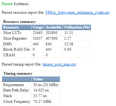
Before you generate HDL code, in the HDL Workflow Advisor > Set Target Frequency window, specify the Target Frequency as 20.
HDL Coder synthesizes the HDL code on the target platform and generates area and timing reports for your design based on the target device that you specify. You can run logic synthesis for a specified FPGA device and get the synthesis reports. For details about the HDL code generation and synthesis of code, see Generate FPGA Bitstream for Two-Phase DC-DC Converter with Tunable Run-Time Parameters.