Main Content

gerberWrite

Generate Gerber files

Description

gerberWrite(designobject) creates a Gerber file from PCB specification files, such as PCBWriter object or pcbStack object.

Note

To create associated files, run any of the analysis functions such as show, impedance, pattern etc. on the antenna before running the gerberWrite function.

gerberWrite(designobject,rfconnector) creates Gerber file using specified RF connector.

gerberWrite(designobject,writer) creates a Gerber file using specified PCB writer services.

gerberWrite(designobject,writer,rfconnector) creates a Gerber file using specified PCB writer and connector services.

[a,g] = gerberWrite(designobject,writer,rfconnector) creates a Gerber file using specified PCB writer and connector services.

Note

You can only use output arguments if the designobject is a pcbStack object.

example

Examples

collapse all

Create a patch antenna with FR4 as a dielectric material using pcbStack object.

p = pcbStack;
d = dielectric("FR4");
d.Thickness = p.BoardThickness;
p.Layers = {p.Layers{1},d,p.Layers{2}};
p.FeedLocations(3:4) = [1 3];
show(p)

Figure contains an axes object. The axes object with title pcbStack antenna element, xlabel x (mm), ylabel y (mm) contains 8 objects of type patch, surface. These objects represent PEC, feed, FR4.

Use a Cinch SMA for feeding the antenna. Use the Mayhew Labs PCB viewer as the 3-D viewer. Change the file name of the Mayhew Writer services to antenna_design_file.

C = PCBConnectors.SMA_Cinch;
W = PCBServices.MayhewWriter;
W.Filename = 'antenna_design_file';

Generate the Gerber-format files.

[A,g] = gerberWrite(p,W,C)
A = 
  PCBWriter with properties:

                        Design: [1x1 struct]
                        Writer: [1x1 PCBServices.MayhewWriter]
                     Connector: [1x1 PCBConnectors.SMA_Cinch]
           UseDefaultConnector: 0
    ComponentBoundaryLineWidth: 8
         ComponentNameFontSize: []
            DesignInfoFontSize: []
                          Font: 'Arial'
                     PCBMargin: 5.0000e-04
                    Soldermask: 'both'
                   Solderpaste: 1

   See info for details
g = 
'/tmp/Bdoc24b_2679053_1419063/tpa45d4ded/antenna-ex85477975/antenna_design_file'

Create a coplanar inverted F antenna.

fco = invertedFcoplanar(Height=14e-3,GroundPlaneLength=100e-3,...
                  GroundPlaneWidth=100e-3);

Use this antenna to create a pcbStack object.

p = pcbStack(fco)
p = 
  pcbStack with properties:

              Name: 'Coplanar Inverted-F'
          Revision: 'v1.0'
        BoardShape: [1×1 antenna.Rectangle]
    BoardThickness: 0.0013
            Layers: {[1×1 antenna.Polygon]}
     FeedLocations: [0 0.0500 1]
      FeedDiameter: 5.0000e-04
      ViaLocations: []
       ViaDiameter: []
      FeedViaModel: 'strip'
       FeedVoltage: 1
         FeedPhase: 0
         Conductor: [1×1 metal]
              Tilt: 0
          TiltAxis: [1 0 0]
              Load: [1×1 lumpedElement]

figure
show(p)

Figure contains an axes object. The axes object with title pcbStack antenna element, xlabel x (mm), ylabel y (mm) contains 3 objects of type patch, surface. These objects represent PEC, feed.

Use an SMA_Cinch as an RF connector and Mayhew Writer as a 3-D viewer.

c = PCBConnectors.SMA_Cinch
c = 
  SMA_Cinch with properties:

                    Type: 'SMA'
                     Mfg: 'Cinch'
                    Part: '142-0711-202'
              Annotation: 'SMA'
               Impedance: 50
               Datasheet: 'https://belfuse.com/resources/Johnson/drawings/dr-142-0711-202.pdf'
                Purchase: 'https://www.digikey.com/product-detail/en/cinch-connectivity-solutions-johnson/142-0711-202/J10154TR-ND/3587681'
               TotalSize: [0.0071 0.0071]
           GroundPadSize: [0.0024 0.0024]
       SignalPadDiameter: 0.0017
         PinHoleDiameter: 0.0013
           IsolationRing: 0.0041
    VerticalGroundStrips: 1

   Cinch 142-0711-202 (Example Purchase)

s = PCBServices.MayhewWriter
s = 
  MayhewWriter with properties:

               BoardProfileFile: 'legend'
          BoardProfileLineWidth: 1
                 CoordPrecision: [2 6]
                     CoordUnits: 'in'
              CreateArchiveFile: 0
                 DefaultViaDiam: 3.0000e-04
             DrawArcsUsingLines: 1
                 ExtensionLevel: 1
                       Filename: 'untitled'
                          Files: {}
         IncludeRootFolderInZip: 0
                   PostWriteFcn: @(obj)sendTo(obj)
    SameExtensionForGerberFiles: 0
                    UseExcellon: 1

Create an antenna design file using PCBWriter.

PW = PCBWriter(p,s,c)
PW = 
  PCBWriter with properties:

                        Design: [1×1 struct]
                        Writer: [1×1 PCBServices.MayhewWriter]
                     Connector: [1×1 PCBConnectors.SMA_Cinch]
           UseDefaultConnector: 0
    ComponentBoundaryLineWidth: 8
         ComponentNameFontSize: []
            DesignInfoFontSize: []
                          Font: 'Arial'
                     PCBMargin: 5.0000e-04
                    Soldermask: 'both'
                   Solderpaste: 1

   See info for details

Use the gerberWrite function to generate gerber files from the antenna design files. Send the generated files to the Mayhew writer manufacturing service.

gerberWrite(PW)

The default folder containing the gerber files is named "untitled" and is located in your MATLAB folder. Running this example automatically opens up the Mayhew Labs PCB manufacturing service in your internet browser.

Drag and drop all your files from the "untitled" folder.

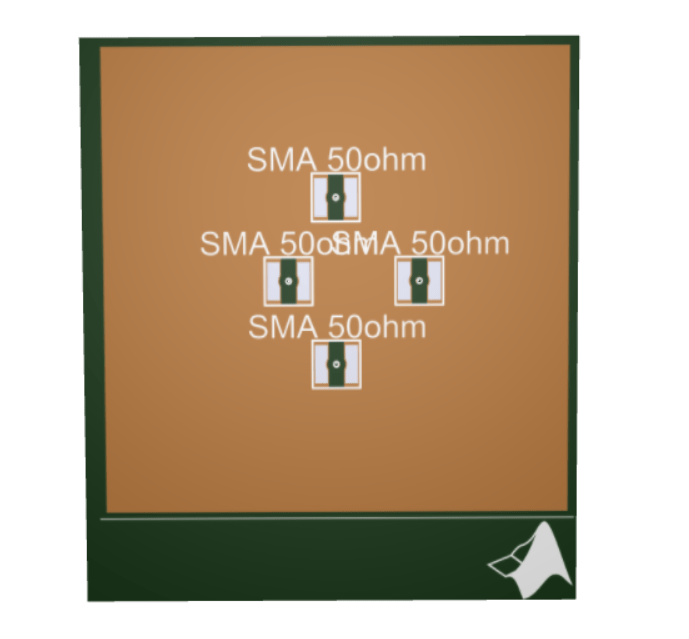
Click Done to view your Antenna PCB.

Design a patch antenna.

p = design(patchMicrostrip,3.5e9);
p.Width = p.Length;
p.Substrate = dielectric("FR4");

Create a stack representation of the patch antenna.

pb = pcbStack(p);
pb.FeedLocations = [pb.FeedLocations;-.007 0 1 3;0 .007 1 3;0 -.007 1 3];

Pick a connector for the feed locations.

C = SMA_Cinchcustom1;

Pick a manufacturing service.

Wr = PCBServices.MayhewWriter;

Create a Gerber file and generate it.

A = PCBWriter(pb,Wr,C);
gerberWrite(A) 

Create a probe-fed microstrip patch antenna with four ports.

p = design(patchMicrostrip(Substrate=dielectric("FR4")),3.5e9);
p.Width = p.Length;
pb = pcbStack(p);
pb.FeedLocations = [pb.FeedLocations;-0.007 0 1 3;0 0.007 1 3;0 -0.007 1 3];
figure
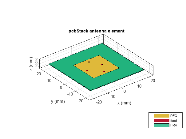
show(pb)

Figure contains an axes object. The axes object with title pcbStack antenna element, xlabel x (mm), ylabel y (mm) contains 17 objects of type patch, surface. These objects represent PEC, feed, FR4.

Pick a manufacturing service.

Wr = PCBServices.MayhewWriter;
Wr.Filename = 'Microstrip antenna-4ports';

Pick a connector for the feed locations.

C = SMA_Cinchcustom1;

Create a Gerber file and generate it.

A = PCBWriter(pb,Wr,C);
A.Soldermask = 'neither';
gerberWrite(A) 

Generate Gerber files with no connectors.

Create a microstrip antenna with FR4 dielectric substrate.

p = patchMicrostrip(Substrate=dielectric("FR4"));
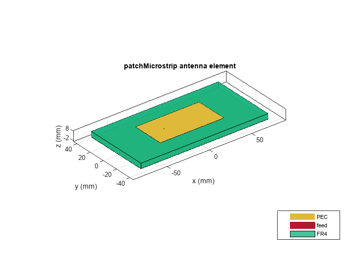
show(p)

Figure contains an axes object. The axes object with title patchMicrostrip antenna element, xlabel x (mm), ylabel y (mm) contains 6 objects of type patch, surface. These objects represent PEC, feed, FR4.

Create a PCB stack of this antenna.

pb = pcbStack(p);

Create an antenna design file using PCBWriter object.

s = PCBServices.MayhewWriter;
s.Filename = 'patchM';
PW = PCBWriter(pb,s);

Set the default connector to false and write the antenna to a Gerber file.

PW.UseDefaultConnector = 0;
gerberWrite(PW)

Input Arguments

collapse all

Antenna design geometry file, specified as a pcbStack object or PCBWriter object.

Example: p1 = pcbStack creates a PCB stack object.p1 gerberWrite(p1) creates a Gerber file using p1.

Example: p1 = pcbStack creates a PCB stack object.p1 a = PCBWriter(p1), creates a PCBWriter object, a. gerberWrite(a), creates a Gerber file using a.

RF connector type, specified as a PCBConnector object.

Example: c = PCBConnectors.SMA_Cinch;gerberWrite(p1,c) uses SMA_Cinch RF connector at the feedpoint.

PCB service, specified as a PCBServices object.

Example: s =PCBServices.MayhewWriter;gerberWrite(p1,s) uses Mayhew Labs PCB service to create and view the PCB design.

Output Arguments

collapse all

Note

You can only use output arguments if the designobject is a pcbStack object.

PCBWriter object that generated the Gerber files, returned as an object.

Path to generated Gerber files folder, returned as character vector.

Version History

Introduced in R2017b