Transmit and Receive Signals Using DDR4 on RFSoC Template
The Transmit and Receive Signals Using DDR4 on RFSoC template provides a reference model for developing communication and radar applications that use DDR4 memory on RFSoC devices. This template serves as a starting point for designing your own transmitter and receiver algorithms and deploying them on RFSoC hardware. Use this template to transmit and receive large data sets by using the external DDR4 memory connected to the FPGA.
You can use this template to emulate waveforms, analyze signals, capture live radio frequency (RF) samples, and perform offline analysis. Capture received data in the DDR4 memory and read it back from MATLAB® for offline analysis. Before validating the receiver device under test (DUT), you can validate the receive path functionality of the RF Data Converter block by bypassing the receiver DUT in the template model.
Create SoC Model Using Template
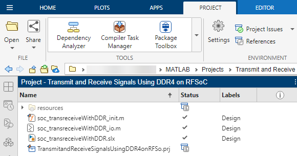
To get started with the SoC model for designing an RFSoC-enabled communication or radar application, create a project by using the template.
On the MATLAB Home tab, click Simulink. Alternatively, at the command line, enter:
simulink
On the Simulink® Start Page, scroll down to the SoC Blockset Support Package for AMD FPGA and SoC Devices section. Select the Transmit and Receive Signals Using DDR4 on RFSoC template and save the project. A project folder opens in your workspace containing:
soc_tansreceiveWithDDR.slx— SoC model for the project.soc_transreceiveWithDDR_init.m— File containing the initialization function for the model. This function sets the model-wide parameters derived based on the specified sample rate.soc_transreceiveWithDDR_io.m— Host interface script for the SoC design. This script contains the DUT ports and interface mapping information. Use this script to access the board memory, DUT registers, and AXI4-Stream interfaces from MATLAB. For more information about the host interface script, see Host Interface Script Files (HDL Coder).
In the
soc_tansreceiveWithDDR.slxmodel, in theTransmit and Receivesubsystem, navigate to the subsystems markedTx DUTin theTx Pathsubsystem, orRx DUTin theRx Pathsubsystem. These subsystems are highlighted for easy detection. Replace the template blocks with your own algorithm model.Add your transmitter and receiver algorithms in the transmitter and receiver DUTs, respectively, in the
Trasmit and Receivesubsystem.
Required Products
DSP HDL Toolbox™
DSP System Toolbox™
HDL Coder™
SoC Blockset™ Support Package for AMD FPGA and SoC Devices
Template Structure
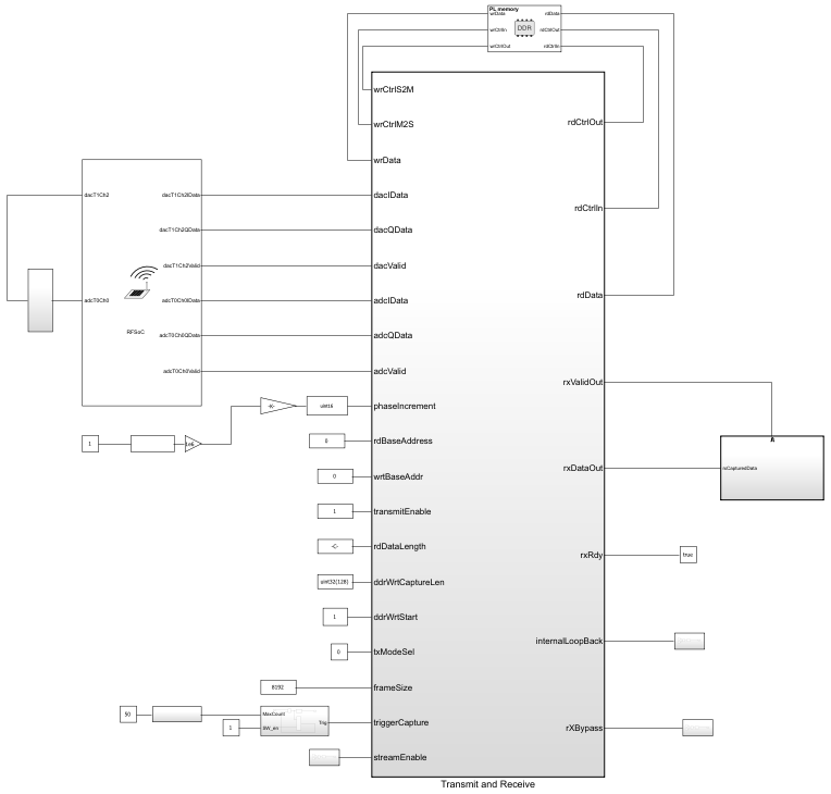
In the Transmit and Receive Signals Using DDR4 on RFSoC template, the RF Data
Converter block connects the Transmit and Receive
subsystem and provides an RF I/O interface. The Transmit and Receive
subsystem implements the transmitter and receiver algorithms. The AXI4 Random Access
Memory block connects the Transmit and Receive subsystem
to the DDR4 memory through AXI4 manager interfaces.
Transmit Path
The Tx Path subsystem includes the Tx DUT and
DDR Transmit Repeat subsystems and connects to the
digital-to-analog converter (DAC) in the RF Data Converter block.
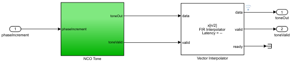
The
Tx DUTsubsystem generates a sinusoidal waveform by using the NCO block and forwards it to the FIR Interpolator block, which upsamples the signal before sending it to the DAC.The
DDR Transmit Repeatsubsystem reads stored waveform samples from the DDR4 memory and repeatedly sends them to the DAC by using transmit repeat logic.
The transmitted data comes from either the DDR4 memory or the
NCO-generated sine wave, based on the txModeSel control input port. A
multiport switch selects the appropriate source and forwards it to the DAC.
This template stores a simple sine waveform in the DDR4 memory by default. You can
write any custom waveform to the DDR4 memory by using the
soc_transreceiveWithDDR_io.m script.
In the RF Data Converter block:
The DAC interpolates the input data by the factor specified in the block mask.
The DAC output is looped back to the analog-to-digital converter (ADC) input.
The ADC decimates the input data by the factor specified in the block mask and outputs it to the receive path.
Receive Path
The Rx Path subsystem receives RF data from the ADC and downsamples
it by using the FIR Decimator block before sending it to the Rx
DUT, BRAM Trigger Capture, and DDR Data
Capture subsystems.
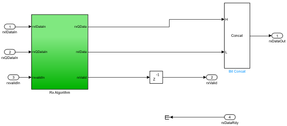
The
Rx DUTsubsystem implements the receiver algorithm (a simple pass-through in this template).The
BRAM Trigger Capturesubsystem writes the incoming data to BRAM by using trigger and capture logic.The
DDR Data Capturesubsystem writes the incoming data to the DDR4 memory.
You can use the DDR Data Capture subsystem to store
the received data in the DDR4 memory and then read the data from the DDR4 memory for
offline analysis. To write the received data to DDR4, uncomment the section in the
soc_transreceiveWithDDR_io.m script that writes the ADC samples
to DDR.
The Rx Bypass subsystem selects the data forwarded to the receiver
output. It chooses either the BRAM data or the Rx DUT output based on
the value of the rxBypass control input port. Before validating the
receiver DUT, you can validate the receive path functionality of the RF Data
Converter block by bypassing the Rx DUT subsystem. The
frameSize input port specifies the size of the data to read from
BRAM.
Customization and RF Configuration
Use this template as a starting point and replace the Tx DUT and
Rx DUT subsystems in the Tx Path and
Rx Path subsystems, respectively, with your own transmitter and
receiver algorithms.
The RF Data Converter block in this template is configured with:
A custom RF interface consisting of one DAC (dacT1Ch2) and one ADC (adcT0Ch0)
An I/Q digital interface
Two samples per clock cycle
A looped-back RF path
If you want to use different data for the receiver, you can remove the loop back and provide your desired input data to the ADC.
Plotting and Analysis
The template reads the received data from the Transmit Receive
subsystem and performs additional processing in the PlotData subsystem.
To view simulation results, double-click the Time Scope block.
To plot received data, double-click the receiverData block.
Modify Project
Modify Transmitter DUT
In the soc_tansreceiveWithDDR.slx model, in the
Transmit and Receive subsystem, open the Tx
Path subsystem. The Tx DUT subsystem represents
user code and is highlighted in green. Replace the NCO Tone block
located in the Tx DUT subsystem with your desired transmitter
algorithm.
Modify Receiver DUT
In the soc_tansreceiveWithDDR.slx model, in the
Transmit and Receive subsystem, open the Rx
Path subsystem. The Rx DUT subsystem represents
user code and is highlighted in green. Replace the Rx Algorithm block
located in the Rx DUT subsystem with your desired receiver
algorithm.