Get Started with SoC Blockset
This example shows how to get started with deploying an algorithm on an SoC hardware board using MATLAB® and Simulink® with SoC Blockset™. This example deploys a single algorithm using two distinct workflows: the IP core generation workflow and the SoC builder workflow. This step-by-step approach helps you choose the workflow that best fits your project requirements and hardware, making it easier to integrate and deploy your algorithms on SoC platforms.
Supported Hardware Platforms
AMD® Zynq® ZC706 evaluation kit
AMD Zynq UltraScale+™ MPSoC ZCU102 Evaluation Kit
AMD Zynq UltraScale+ MPSoC ZCU106 Evaluation Kit
AMD Zynq UltraScale+ RFSoC ZCU111 Evaluation Kit
AMD Zynq UltraScale+ RFSoC ZCU208 Evaluation Kit
AMD Zynq UltraScale+ RFSoC ZCU216 Evaluation Kit
AMD Zynq UltraScale+ RFSoC DFE ZCU670 Evaluation Kit
ZedBoard™ Zynq-7000 Development Board
This example uses ZedBoard as the default hardware board.
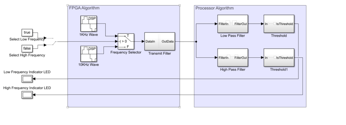
Algorithm
This example uses an algorithm in which the FPGA generates two sine waves at frequencies of 1 kHz and 10 kHz. A switch mechanism in the FPGA selects one of these sine waves and sends the selected signal to the processor. The processor uses a lowpass filter and a highpass filter to analyze the incoming signal and determine whether the transmitted sine wave is low or high frequency. Based on the filter outputs, the processor detects which sine wave is sent. After identifying the transmitted frequency, the processor sends the detection result back to the FPGA. The FPGA uses this information to control two LEDs: one indicates low frequency and the other indicates high frequency. The LED corresponding to the detected frequency glows.
Deploy Algorithm Using IP Core Generation Workflow
open_system('hdl_gettingStarted');
Follow these steps to deploy the algorithm by using the IP core generation workflow.
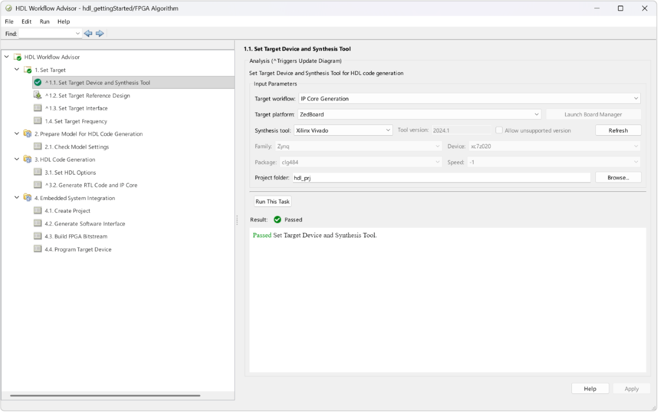
1. Open HDL Workflow Advisor by clicking Workflow Advisor on the HDL Code tab of the Simulink toolstrip.
2. In step 1.1, set Target workflow to IP Core Generation and select your target platform.
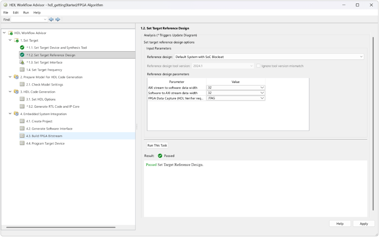
3. In step 1.2, set Reference design to Default System with SoC Blockset.
4. In step 1.3, update the target platform interface table. Add both the AXI master and AXI slave interfaces to use this reference design. If any of these interfaces is missing, add dummy ports for them.
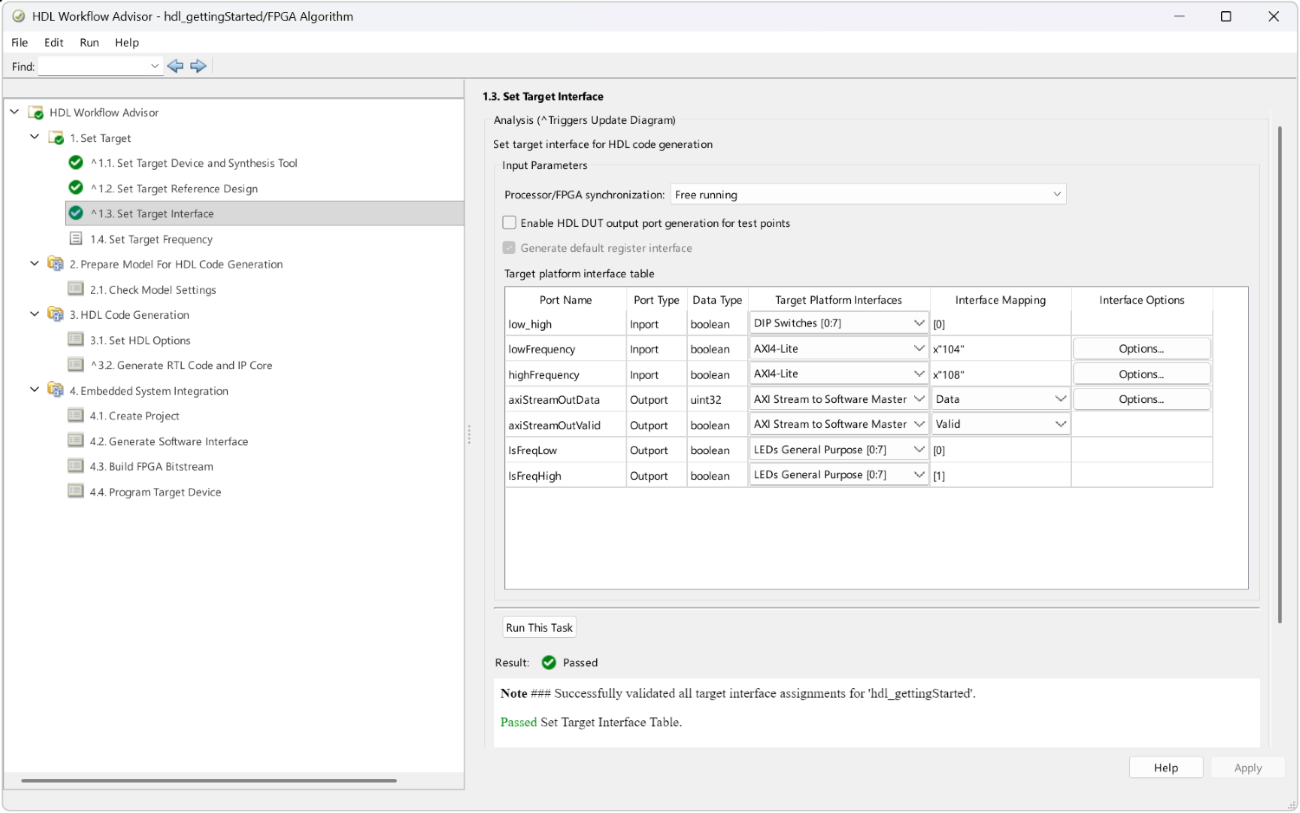
5. Right-click step 4.4 and click Run to selected Task to complete all remaining steps, build the bitstream, and program the hardware board.
Verification on Hardware Board
This example uses FPGA I/O for hardware verification. Set the general purpose DIP switch0 on the hardware to off to select high frequency. Run the host interface script hdl_gettingStarted_interface.m. Based on the selected frequency, the general purpose LED1 on the hardware board glows. Similarly, set the DIP switch0 to on to select low frequency and run the host interface script again. The general purpose LED0 on the hardware board glows.
Deploy Algorithm Using SoC Builder Workflow
Follow these steps to deploy the algorithm by using the SoC builder workflow. Steps 1 to 3 explain how to create the top model and referenced FPGA and processor models from the algorithm.
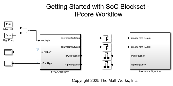
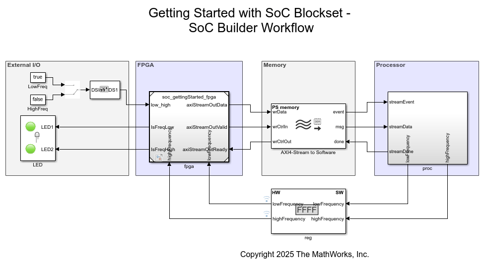
1. Identify the interfaces required for the algorithm. The switch and display blocks serve as external input and external output for the FPGA, respectively. The path from the FPGA to the processor is the data stream. The path from the processor to the FPGA is the registered signal.
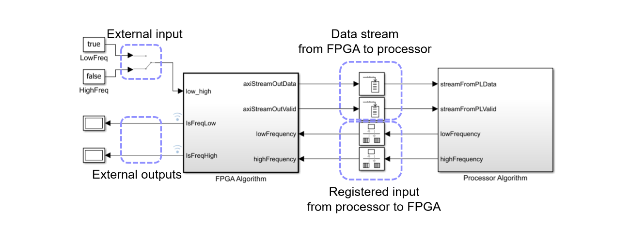
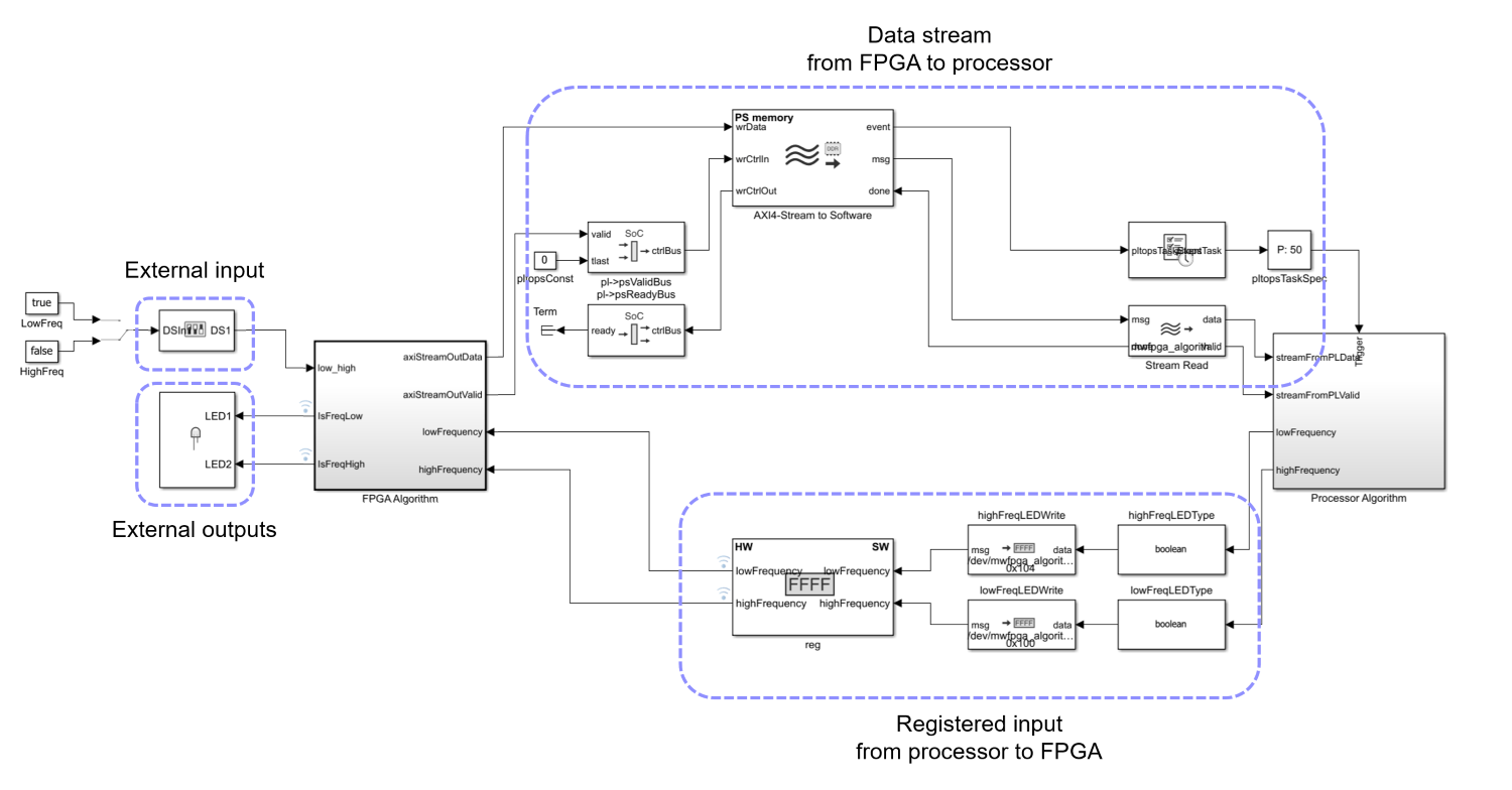
2. Replace the external input with a DIP Switch block. Replace external outputs with LED blocks. Replace the data stream from the FPGA to the processor with AXI4-Stream to Software, Bus Creator, Stream Read, and Task Manager blocks. Replace the registered input from the processor to the FPGA with Register Channel, Register Write, and Data Type Conversion blocks.
3. Group the blocks that run on the FPGA and create an FPGA reference model. Group the blocks that run on the processor and create a processor reference model.
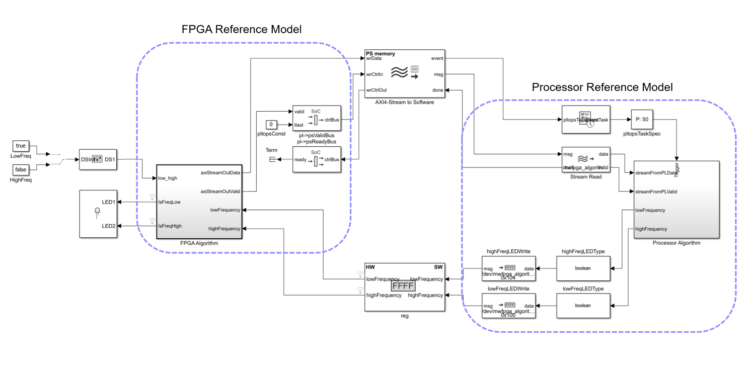
The model now resembles an SoC Blockset top model, as this figure shows.
open_system('soc_gettingStarted_top');
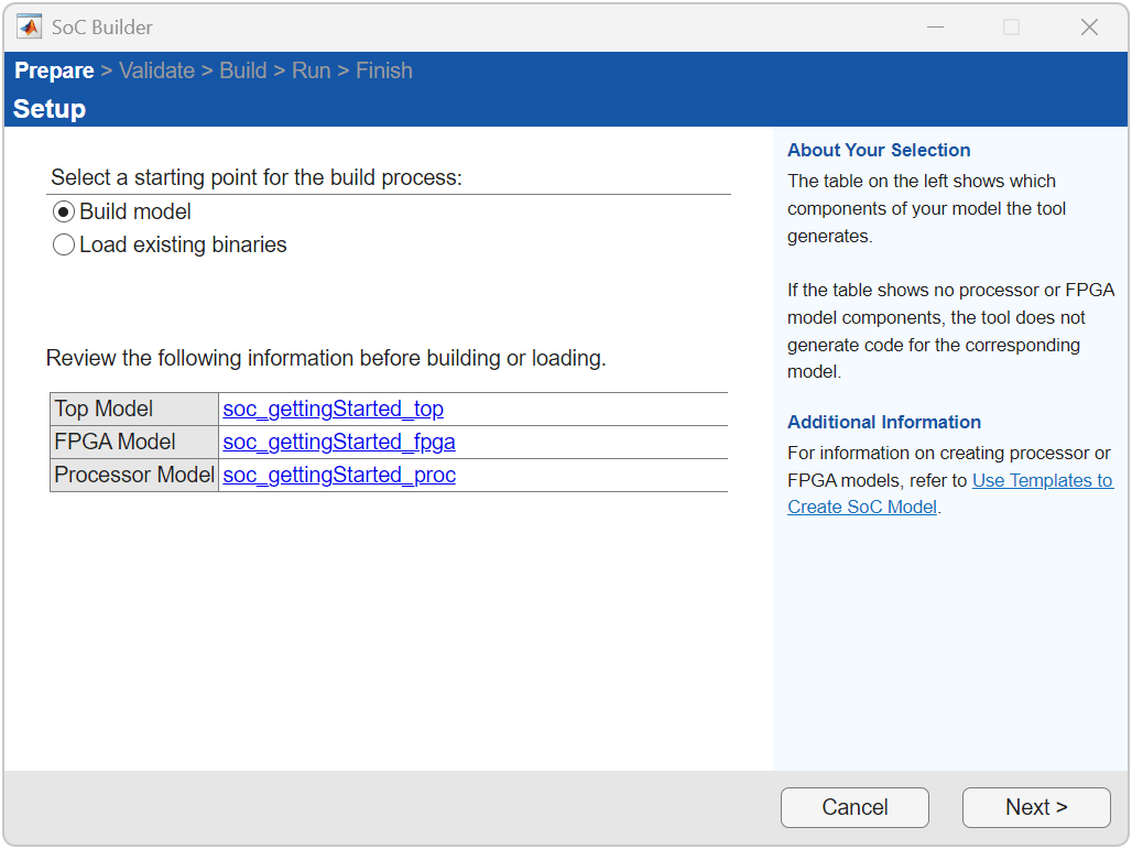
4. Open SoC Builder by clicking Configure, Build & Deploy on the System on Chip tab of the Simulink toolstrip.
5. On the Setup screen, select Build model. Click Next.
6. On the Select Build Action screen, select Build, load, and run. Clear Manually configure build process. Click Next.
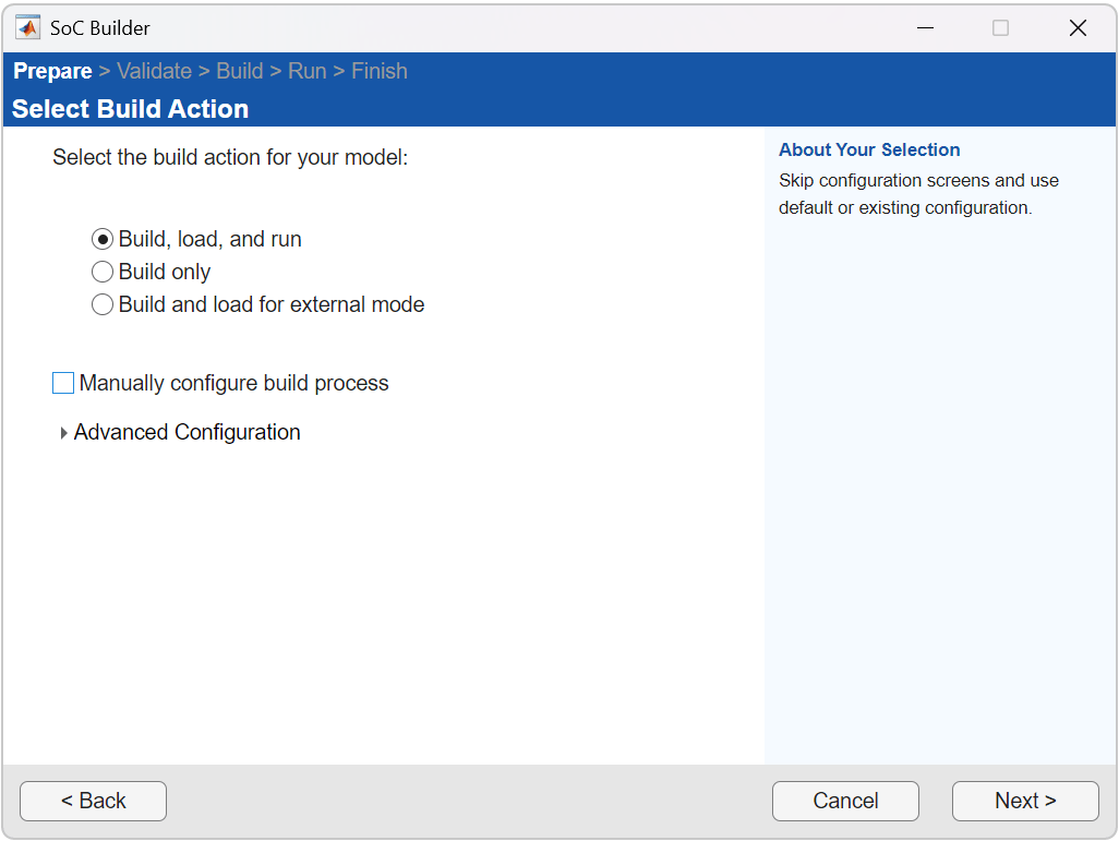
Doing so generates a bitstream for your FPGA design and a compiled executable for your processor, loads it on the hardware, and starts the application on the hardware.
Verification on Hardware Board
The DIP Switch block gives you the location of the frequency control switch. The LED block shows the locations of the frequency indicator LEDs on the hardware. You can change the frequency control switch and verify that the corresponding frequency indicator LED glows on the hardware.
Choose Workflow
This section helps you decide when to choose the IP core generation workflow or the SoC builder workflow.
IP Core Generation Workflow
Best when you want to integrate your FPGA algorithm into a fixed reference design with predefined interfaces
Suitable for rapid prototyping and when your interface requirements match the available reference designs
SoC Builder Workflow
Recommended when you need custom interfaces or greater control over hardware-software partitioning
Useful for advanced designs that require managing multiple custom interfaces or integrating with a larger SoC system
Provides full flexibility to modify and extend the reference design per your requirements
bdclose('hdl_gettingStarted');
bdclose('soc_gettingStarted_top');