Add Custom Board Definition for FPGA-in-the-Loop Using JTAG
This example shows how to support FPGA-in-the-loop (FIL) simulation on a custom FPGA board using JTAG. If HDL Verifier® does not support your FPGA board by default, create a custom board definition in the FPGA Board Manager. This example uses the AMD® Zynq™ 7000 SoC ZC706 evaluation kit with the JTAG interface.
Requirements
See FPGA Board Requirements to verify that your board and JTAG interface are supported for customization.
Before you begin, gather the following information:
JTAG chain position, instruction register (IR), USERCODE, and TCK clock frequency
FPGA input clock frequency, clock type, pin number, and I/O standard
(Optional) Reset pin number, active level, and I/O standard
Find the details in the board specification and the Boundary Scan Description Language (BSDL) model file provided by the vendor. For this example, see:
Create Board Definition
New FPGA Board Wizard
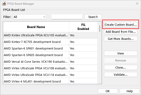
Open the FPGA Board Manager by entering the following command at the MATLAB® prompt:
fpgaBoardManager
Click Create Custom Board to open the New FPGA Board wizard.
Basic Information
In the Basic Information pane:
Set Board Name to
My AMD ZC706 Board.Set Vendor to
AMD.Set Family to
Zynq.Set Device to
xc7z045.Set Package to
ffg900.Set Speed to
-2.Set JTAG Chain Position to 2.
Click Next to continue.
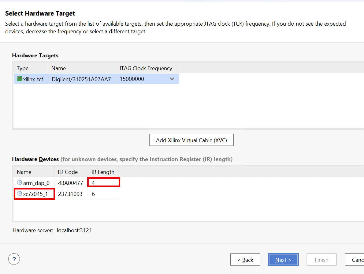
You can determine the JTAG chain position by using your vendor’s tool. Connect the board to your computer with a JTAG cable and open the Vivado® Hardware Manager. In the list of detected hardware devices, locate the FPGA device (xc7z045_1). Since it appears on the second row, the JTAG chain position is 2.
Interfaces
In the Interfaces pane:
Select the FIL Interface check box.
Select JTAG for the PHY interface type.
Set Clock Frequency to
200.Set Clock Type to
Differential.Set Clock_P Pin Number to
H9.Set Clock_N Pin Number to
G9.Set Clock I/O Standard to
LVDS.Set Reset Pin Number to
A8.Set Active Level to
Active-High.Set Reset I/O Standard to
LVCMOS15.
You can find these clock and reset details in the ZC706 Evaluation Board for the Zynq-7000 XC7Z045 SoC User Guide.
Click Next to continue.
FIL I/O
In the FIL I/O pane:
Set Sum of IR length before to
4because the IR length of the device before the FPGA,arm_dap_0, is 4. You can find this value in the Vivado Hardware Manager.Set Sum of IR length after to
0because the FPGA is the last device in the JTAG chain.
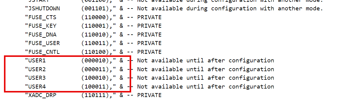
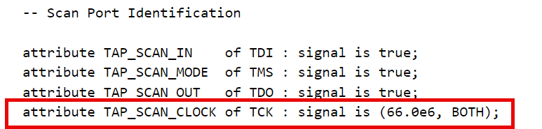
The information of JTAG USERCODE and TCK clock frequency can be found in the BSDL Models for Versal, Zynq UltraScale+, and Zynq 7000 SoCs. After unzipping the downloaded files, find the .bsd file that matches your FPGA device. For this example, open the file named xc7z045_ffg900.bsd. Inside this file, you can find the entries for USERCODE and TCK frequency, such as:
To configure these settings, expand Advanced Options in the FIL I/O pane:
Set User1 Instruction to
000010.Set User2 Instruction to
000011.Set User3 Instruction to
100010.Set User4 Instruction to
100011.Set JTAG Clock Frequency (MHz) to
66.
Click Next to continue.
Validation
You can validate your board customization by running an FPGA-in-the-loop (FIL) simulation test. To perform this validation, make sure that:
The AMD Vivado® tool is installed and on the MATLAB path. See AMD Usage Requirements for the recommended version.
The ZC706 board is connected to your computer via a JTAG cable.
To run this test:
Select the Run FPGA-in-the-Loop test check box and then select the Include FPGA board in the test check box.
Click Run Selected Test(s). The test can take up to 30 minutes to complete.
Click Finish to exit the New FPGA Board wizard. When prompted, choose a location to save the FPGA board definition file and click Save. The new board now appears in the FPGA Board Manager. Click OK to close the FPGA Board Manager.
Run FIL Simulation on Custom Board
You can run the FIL simulation on the custom board by using either the FIL wizard or HDL Workflow Advisor.
Using FIL Wizard
Start the FIL wizard by entering the following command at the MATLAB prompt:
filWizard
Select My AMD ZC706 Board from the Board Name list for FPGA-in-the-loop simulation.
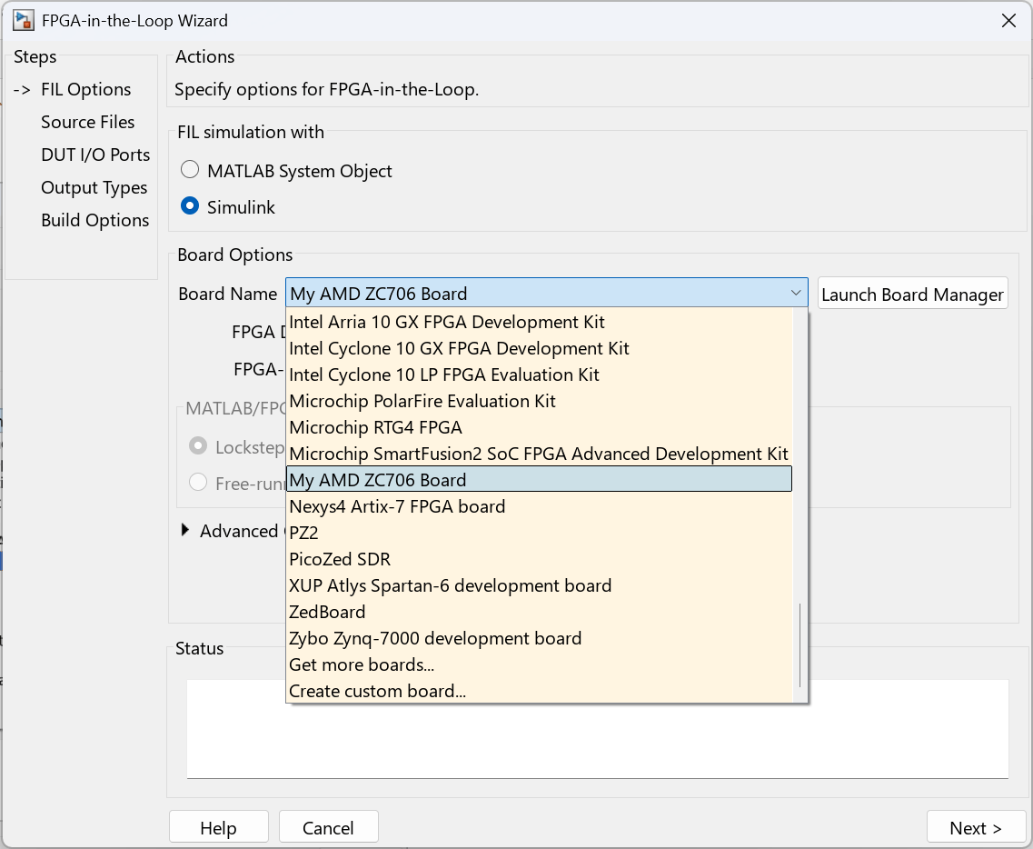
Then follow the steps to generate an FIL block or System object™ and run the FIL simulation. For example:
Using HDL Workflow Advisor
Start HDL Workflow Advisor from your Simulink model or MATLAB code.
Set Target workflow to FPGA-in-the-Loop, and then select My AMD ZC706 Board from the Target platform list for FPGA-in-the-loop simulation.
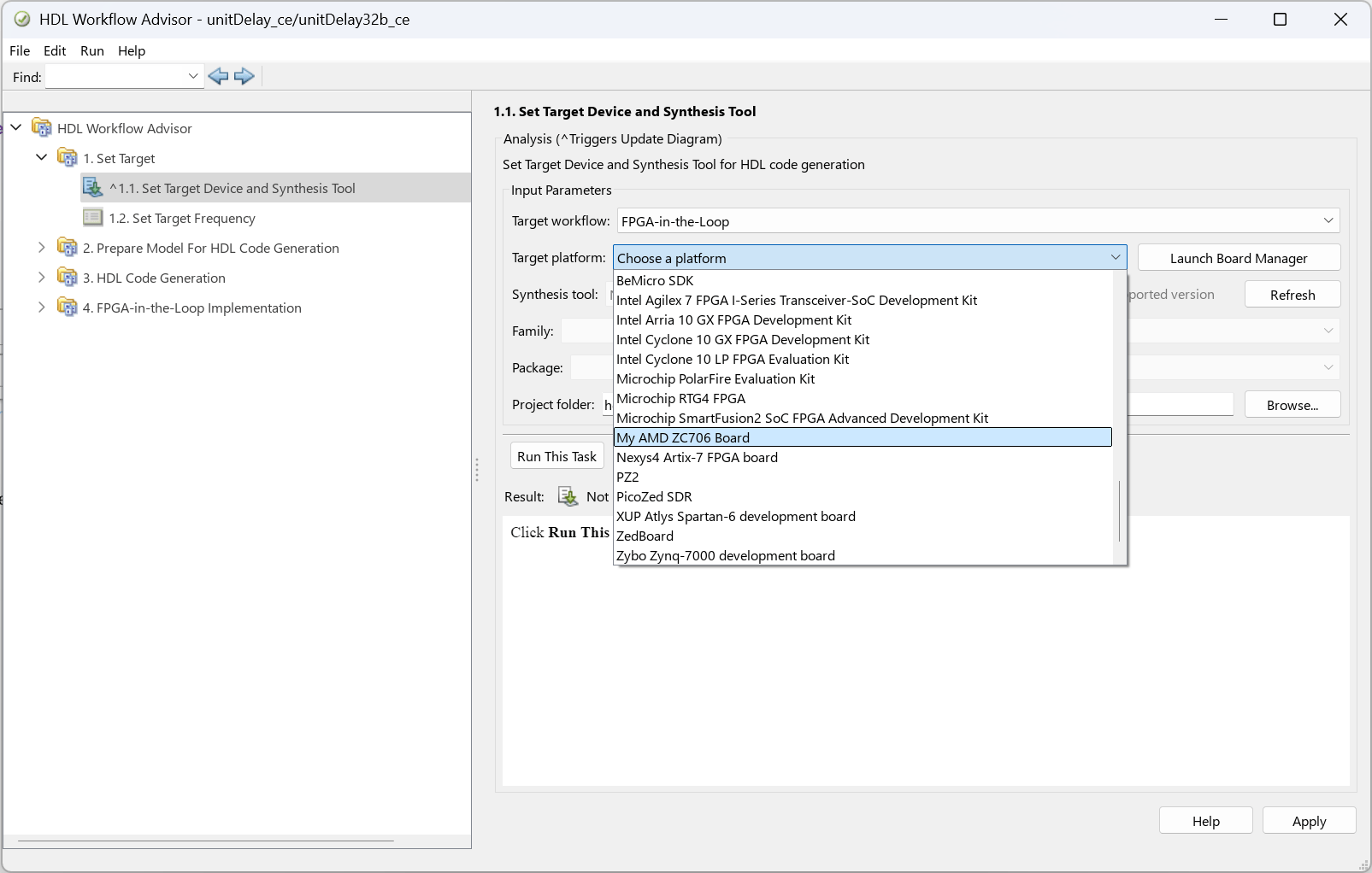
Then follow the steps to run the FIL simulation. For example: