Modeling 5G Millimeter Wave Beamformer Integrated Circuits
By Cecile Masse, Otava Inc.
When designing phased array systems, RF engineers need to verify signal integrity and compliance with the 3GPP standard specifications as early as possible. At the same time, they must ensure that the design meets the practical needs of their customers in terms of phased array size, quality of the antenna pattern, and sensitivity to various parameter values.
Once the antenna, beamformer devices, and transceiver hardware are assembled, engineers can run experiments in over-the-air (OTA) test chambers to characterize their design. However, it is often weeks—or even months, depending on hardware and software development time, as well as product availability—before all the pieces of the radio system become available.
Our team has built a behavioral model of the Otava OTBF103 Beamformer Integrated Circuit (BFIC) that enables engineers to obtain essential performance information by running system-level simulations of their 5G millimeter wave system designs. The model can be simulated across eight transmit channels and eight receive channels in the 24 GHz to 40 GHz range, which spans numerous 5G NR bands. Engineers may combine the model with their own antenna models or use the antenna models included in the testbenches we provide. They can run simulations using their own Simulink® transceiver designs, transceiver models included in the testbench, or signal data captured from real-world RF systems.
By running comprehensive bits-to-antenna simulations with the BFIC model, engineers can optimize and verify their system designs across a range of RF operating frequencies, variable gain amplifier (VGA) settings, phase shifter settings, and input/out power levels—all before committing to hardware or conducting over-the-air tests using an OTBF103 evaluation board (Figure 1). Once hardware is available, they can continue to use the model to further refine and verify their design.

Figure 1. The Otava OTBF103 evaluation board.
Building the BFIC Model
We began by modeling the transmitter channels, basing the model structure on the BFIC circuit-level behavior. Each TX signal path captures the behavior of the circuit’s power splitter, phase shifter, variable gain amplifier, and output power amplifier, modeled using the RF Blockset™ Power Divider, Phase Shift block, and nonlinear Amplifier block, respectively. The model is based on numerous measurement data sets, including complete S-parameters for the circuit’s input and output ports, collected on the actual BFIC device. As a result, it accurately captures the response of the beamformer over a range of RF parameters, such as center frequency, phase shift, and gain operating point, as well as residual amplitude and phase error.
After verifying a preliminary version of the model, we worked with MathWorks engineers to refine it. We restructured the model more efficiently, grouping impairments and nonlinearities distributed across several elements into one location (Figure 2).
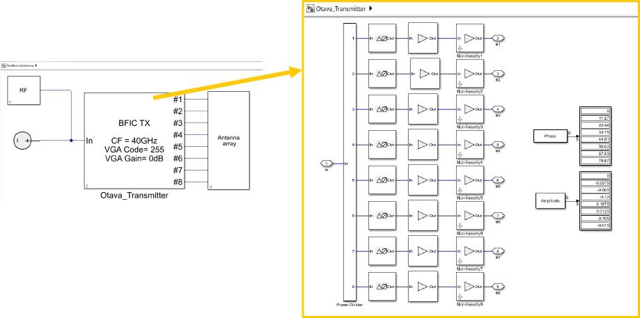
Figure 2. The BFIC transmitter block (left) and its internal structure (right), including variable phase shift and variable gain amplifier elements.
This grouping simplified the model, making it both easier to use and more computationally efficient. It also enabled us to protect our intellectual property, since the restructured model was less like the actual circuit implementation than the initial version had been.
The complete BFIC model includes both transmitter and receiver blocks. The receiver block mirrors its transmitter counterpart, with input signals from eight antenna inputs passing through low-noise amplifiers, variable-gain amplifiers, and phase shifters.
Simulating 5G Millimeter Wave Designs
Otava customers can use our BFIC model in a variety of ways to evaluate their designs. For example, they can simulate not only classic CW RF performance characteristics like gain, IP3, and noise figure, but also apply 5G NR waveforms using the RF Measurement Testbench that we provide (Figure 3).
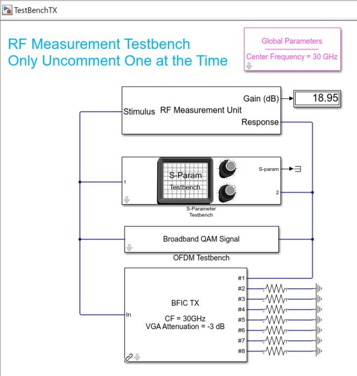
Figure 3. The RF Measurement Testbench.
The default modulated signal is a 100 MHz OFDM signal. The simulation returns a number of key parameters for the radio designer to check compliance with 3GPP standards, such as integrated output power level, ACLR, error vector magnitude (EVM), and constellation diagram (Figure 4).
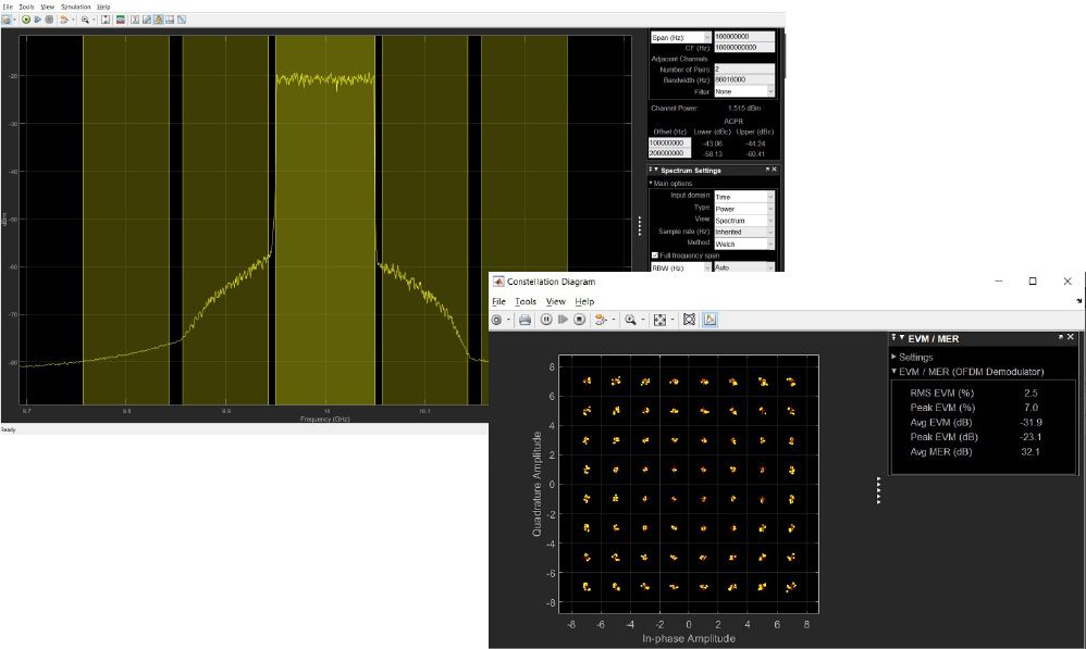
Figure 4. Single-channel ACLR plot and EVM for a standard 100 MHz OFDM signal.
We also provide testbenches for cosimulating the TX or RX BFIC models with an antenna array model. Users may start with these examples to see how their antenna design performs with the beamformer, validating the antenna radiation pattern, sidelobe or null levels, and Effective Isotropic Radiated Power (EIRP) at the target beam direction and under a variety of operating conditions (Figure 5). The provided Antenna Analysis Testbench implements an array of dipoles or circular patch antennas with Antenna Toolbox™ for the simulation of polar directivity patterns, and calculation of the EIRP as a function of the RF center frequency and beam direction. Users may also modify the testbenches to put in their own custom antenna design, generated using either the MATLAB Antenna Designer application or antenna S-parameter data and a directivity profile extracted from an EM simulation tool.
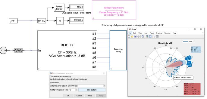
Figure 5. Simulink model including the BFIC transmitter block and a dipole antenna array, with the simulated polar directivity pattern and EIRP (right).
Planned Enhancements
While the offered OTBF103 model is already quite complete for any RF signal chain analysis, we are planning improvements for future versions based on the device’s current and future capabilities. One enhancement under consideration is the addition of multi-bias control. Adding bias control enables engineers to evaluate how their systems perform at reduced power levels. Power consumption has become an important design parameter in 4G cellular radios—even more so in multichannel 5G cellular infrastructure equipment. Understanding how a device may be used to save power under lower traffic load is paramount, and it is important for the model to capture that aspect of device behavior. We also plan to reuse the current model, adapting it to reflect the behavior of upcoming beamformer ICs that are under development.
In the short term, we’ll be offering an end-to-end, over-the-air analysis testbench connecting two MIMO systems. This testbench will be an extension of our antenna array testbenches, making it possible to model a full radio link with beamforming. This setup will account for any custom path loss and allow for signal budget analysis as a function of TX-to-RX beam alignment.
Published 2022